Semiconductor device, manufacturing method therefor and electronic device
A semiconductor and device technology, applied in the field of semiconductor manufacturing technology, can solve the problems of increased diffusion of conductor materials and increased leakage current, and achieve the effects of reducing process cost, reducing leakage current, and increasing formation rate
Active Publication Date: 2015-11-25
SEMICON MFG INT (SHANGHAI) CORP
View PDF6 Cites 4 Cited by
- Summary
- Abstract
- Description
- Claims
- Application Information
AI Technical Summary
Problems solved by technology
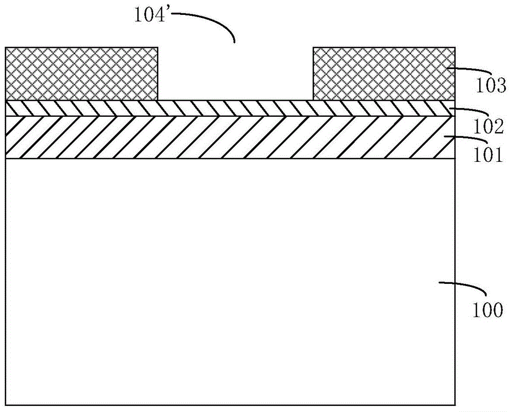
[0004] The upper part of the sidewall of the through-silicon via formed by etching in the prior art usually has an undercut or recess phenomenon, resulting in a very thin barrier layer subse
Method used
View moreImage
Smart ImageViewing Examples


Examples
 PUM
 Abstract
The invention provides a semiconductor device, a manufacturing method therefor and an electronic device. The method comprises steps: a semiconductor substrate is provided, a hard mask laminated structure and a photoresist layer with a pattern of silicon through holes are formed on the semiconductor substrate in order; the photoresist layer is employed as a mask layer, the hard mask laminated structure is etched until the semiconductor substrate is exposed; the semiconductor substrate is etched, and silicon through holes are formed in the semiconductor substrate. Undercutting or recessing at the upper parts of the sidewalls of the formed silicon through holes can be avoided, the leakage current is decreased effectively, the forming speed of silicon through holes is raised, and the technology cost is lowered.
Description
technical field [0001] The invention relates to a semiconductor manufacturing process, in particular to a semiconductor device, a manufacturing method thereof, and an electronic device. Background technique [0002] In the field of consumer electronics, multi-function devices are increasingly favored by consumers. Compared with devices with simple functions, the production process of multi-function devices will be more complicated, such as the need to integrate multiple chips with different functions on the circuit layout. 3D integrated circuit technology. A 3D integrated circuit is defined as a system-level integrated structure that stacks multiple chips in vertical and plane directions to save space. The edge of each chip can lead to multiple pins as needed, and use these pins as needed , The chips that need to be connected to each other are interconnected by metal wires. However, the above method still has many deficiencies, such as the large number of stacked chips, th...
Claims
Login to View More Application Information
Patent Timeline
 IPC IPC(8): H01L21/768
Inventor 伏广才李华乐
Owner SEMICON MFG INT (SHANGHAI) CORP
Features
- R&D
- Intellectual Property
- Life Sciences
- Materials
- Tech Scout
- Unparalleled Data Quality
- Higher Quality Content
- 60% Fewer Hallucinations
Learn More Browse by: Latest US Patents, China's latest patents, Technical Efficacy Thesaurus, Application Domain, Technology Topic, Popular Technical Reports.
© 2025 PatSnap. All rights reserved.Legal|Privacy policy|Modern Slavery Act Transparency Statement|Sitemap|About US| Contact US: help@patsnap.com