Wafer alignment device and semiconductor processing equipment

A wafer calibration and wafer technology, which is applied in semiconductor/solid-state device manufacturing, electrical components, circuits, etc., can solve the problems of large data processing and calibration of processing units, increase the difficulty of implementation, and increase production costs, so as to reduce equipment and Effects of production cost, burden reduction, and contrast enhancement

Active Publication Date: 2018-09-18
BEIJING NAURA MICROELECTRONICS EQUIP CO LTD
View PDF3 Cites 0 Cited by
  • Summary
  • Abstract
  • Description
  • Claims
  • Application Information

AI Technical Summary

Problems solved by technology

The existence of the transition region makes it necessary to search for the real light-dark junction in the subsequent data processing process, that is, to obtain the actual edge position information of the wafer, thus bringing a greater burden on the data processing and calibration of the processing unit
Moreover, since the longer the length of the transition zone, the higher the requirement for the optimization degree of the processing unit, this not only increases the difficulty of implementation, but also increases the hardware cost
[0008] Second, in theory, only when the light receiving assembly 12 is absolutely parallel to the surface of the wafer and the light emitted by the light source is parallel light can the transition zone be avoided. To achieve this, the mounting accuracy and calibration accuracy of the wafer alignment device have to be raised. Higher requirements, thus increasing production costs

Method used


Image

  • Wafer alignment device and semiconductor processing equipment
  • Wafer alignment device and semiconductor processing equipment
  • Wafer alignment device and semiconductor processing equipment

Examples


Embodiment Construction

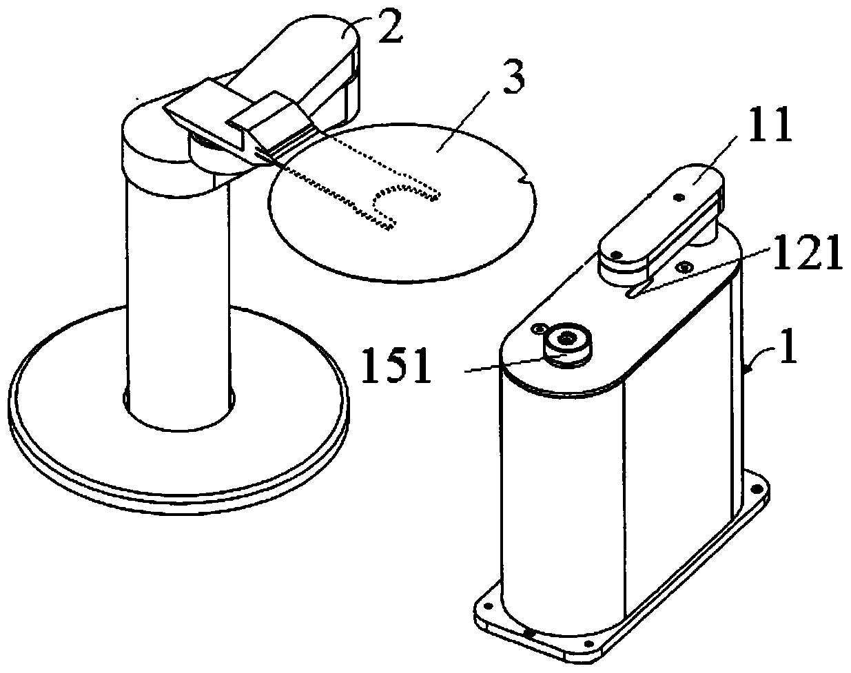
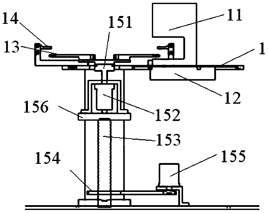
[0031] To enable those skilled in the art to better understand the technical solutions of the present invention, the wafer calibration device and semiconductor processing equipment provided by the present invention will be described in detail below with reference to the accompanying drawings.

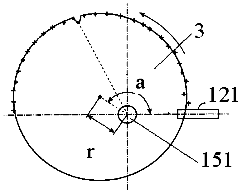
[0032] Please refer to Figure 4A-5B The wafer calibration device includes a box body 20, a carrier, a rotating mechanism, a light source 21, and a light receiving and processing device. Among them, the structure of the carrier is as Figure 4B As shown, it includes four symmetrically distributed carrying arms 24, the four carrying arms 24 are horizontally arranged above the top surface 201 of the box body 20, and the upper surface thereof serves as the carrying surface 241 for carrying the wafer S; and The surface 201 is also provided with four supporting claws 23 surrounding the four carrying arms 24 for supporting the wafer S when the robot is used to load and unload the wafer S. The r...


PUM


Abstract

The invention provides a wafer calibration device and semiconductor processing equipment. The wafer calibration device comprises a load bearing member, a rotating mechanism, a light source and a light receiving and processing device, wherein the load bearing member comprises a load bearing surface used for bearing a wafer; the rotating mechanism is used for driving the load bearing member to rotate; the light source is arranged above the load bearing member and used for transmitting light towards the edge of the load bearing surface; the light receiving and processing device comprises a light receiving assembly, and is used for receiving the light, converting the light into electric signals and sending out the electric signals; and the light receiving assembly is arranged below the load bearing surface, and is located close the position of the load bearing surface. The wafer calibration device provided by the invention can shorten the length of a transition area, thereby not only being capable of reducing the implementation difficulty of software and the hardware cost, but also being capable of reducing requirements for the installation accuracy and the calibration accuracy, and thus being capable of reducing the production cost.

Description

Technical field [0001] The invention relates to the technical field of semiconductor processing, in particular to a wafer calibration device and semiconductor processing equipment. Background technique [0002] In the semiconductor manufacturing process, the wafer to be processed needs to be gradually transferred from the atmospheric environment to the reaction chamber for processes such as etching and deposition. This requires a wafer transfer system composed of a series of atmospheric equipment and vacuum equipment. For example, it is usually necessary to use a manipulator to carry out transfer, fetch and put out operations to realize wafer transfer and loading and unloading. In order to ensure the stability of the process, it is required that the wafer can be accurately transferred to the designated position. Although the theoretical transfer accuracy of the current manipulator can meet the process requirements, in the actual transfer process, it is often due to various facto...

Claims


Application Information

Patent Timeline
Patent Type & Authority Patents(China)
IPC IPC(8): H01L21/68H01L21/67
Inventor 李靖
Owner BEIJING NAURA MICROELECTRONICS EQUIP CO LTD
Why Eureka
Try Eureka