Method and device for triggering operation in information storage type flash memory
A data storage and trigger operation technology, applied in information storage, static memory, read-only memory, etc., can solve the problem of limiting the application range of data storage flash memory, achieve the effect of expanding the application range and overcoming the restriction requirements
- Summary
- Abstract
- Description
- Claims
- Application Information
AI Technical Summary
Problems solved by technology
Method used
Image
Examples
Embodiment 1
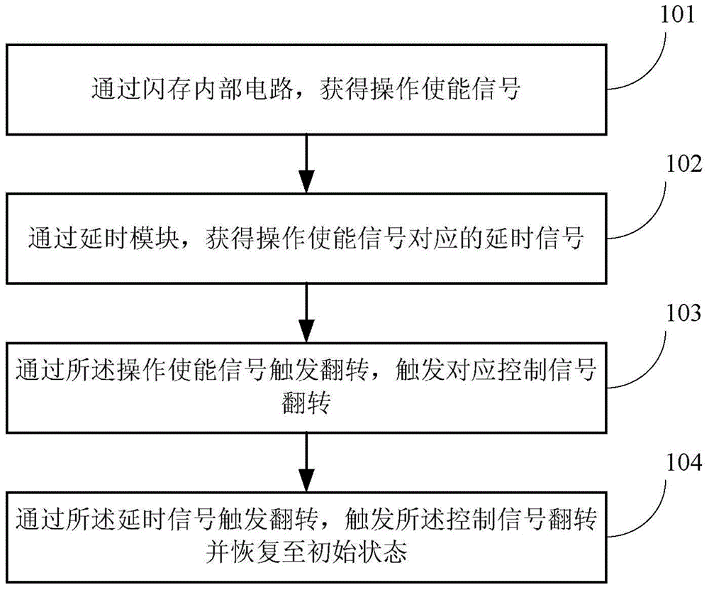
[0027] figure 1 It is a flow chart of a method for triggering an operation in a data storage type flash memory provided by an embodiment of the present invention.
[0028] Such as figure 1 As shown, a method for triggering operations in a data storage type flash memory (hereinafter referred to as flash memory), comprises the following steps:
[0029] 101. Obtain an operation enable signal through an internal circuit of the flash memory.
[0030] Wherein, the operation enable signal includes a read enable signal or a write enable signal. It is worth noting that the read enable signal is loaded from the external read signal to the internal circuit of the flash memory and obtained after processing; while the write enable signal is loaded from the external write signal to the internal circuit of the flash memory and obtained after processing of.
[0031] 102. Obtain a delay signal corresponding to the operation enable signal through the delay module. The length of the delay t...
Embodiment 2
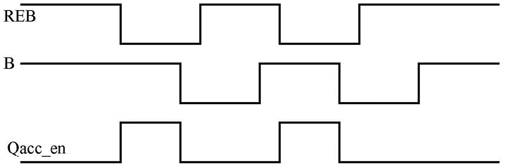
[0039] figure 2 is a timing diagram of a method for triggering operations in a data storage flash memory provided by an embodiment of the present invention.
[0040] Depend on figure 2 As shown, taking the operation enable signal as the read enable signal REB as an example, the method for triggering operation in the data storage flash memory of the present invention can be understood as:
[0041] First, the external read-in signal passes through the internal circuit of the flash memory to generate a corresponding read enable signal REB. Moreover, the read enable signal is in a high level state in an initial state.
[0042] The read enable signal REB passes through the delay module in the internal circuit of the flash memory to obtain the delay signal B of the read enable signal. It should be pointed out here that the delay time of the delay signal B is set according to the internal delay module of the flash memory.
[0043] When the read enable signal REB flips from a hi...
Embodiment 3
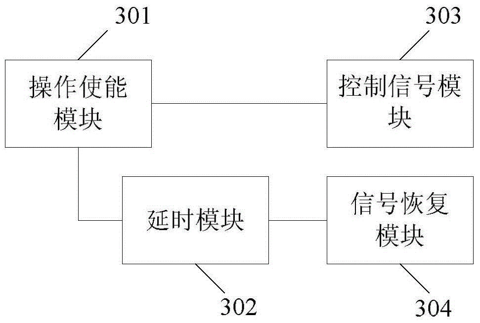
[0048] image 3 It is a schematic structural diagram of a device for triggering operations in a data storage flash memory provided by an embodiment of the present invention.
[0049] Depend on image 3 As shown, a device for triggering operations in a data storage type flash memory includes an operation enabling module 301, a delay module 302, a control signal module 303, and a signal recovery module 304;
[0050] Wherein, the operation enabling module 301 is used for obtaining the operation enabling signal REB / WEB through the internal circuit of the flash memory. The operation enable signal here includes a read enable signal REB and a write enable signal WEB.
[0051] The delay module 302 is configured in the internal circuit of the data storage type flash memory, and is used for obtaining the delay signal B corresponding to the operation enable signal REB / WEB. Here, the delay module 302 comes from the internal circuit of the flash memory, and is used to delay the operatio...
PUM
 Abstract
Description
Claims
Application Information
 - R&D
- Intellectual Property
- Life Sciences
- Materials
- Tech Scout
- Unparalleled Data Quality
- Higher Quality Content
- 60% Fewer Hallucinations
Browse by: Latest US Patents, China's latest patents, Technical Efficacy Thesaurus, Application Domain, Technology Topic, Popular Technical Reports.
© 2025 PatSnap. All rights reserved.Legal|Privacy policy|Modern Slavery Act Transparency Statement|Sitemap|About US| Contact US: help@patsnap.com


