
Display substrate and manufacturing method thereof, and display apparatus

A technology of a display substrate and a manufacturing method, which is applied in the field of display substrate manufacturing and display devices, can solve the problems of IGZO being easily affected by external light, unstable active layer, unstable working performance of thin film transistors, etc.

Active Publication Date: 2015-09-23
BOE TECH GRP CO LTD
View PDF4 Cites 13 Cited by
  • Summary
  • Abstract
  • Description
  • Claims
  • Application Information

AI Technical Summary

Problems solved by technology

[0003] However, when IGZO is used to make the active layer in a thin film transistor, because IGZO is easily affected by external light, such as figure 1 As shown, it will make the active layer unstable, resulting in unstable performance of thin film transistors in the presence of external light

Method used


Image

  • Display substrate and manufacturing method thereof, and display apparatus
  • Display substrate and manufacturing method thereof, and display apparatus
  • Display substrate and manufacturing method thereof, and display apparatus

Examples


Embodiment Construction

[0091] In order to understand the above-mentioned purpose, features and advantages of the present invention more clearly, the present invention will be further described in detail below in conjunction with the accompanying drawings and specific embodiments. It should be noted that, in the case of no conflict, the embodiments of the present application and the features in the embodiments can be combined with each other.

[0092] In the following description, many specific details are set forth in order to fully understand the present invention. However, the present invention can also be implemented in other ways different from those described here. Therefore, the protection scope of the present invention is not limited by the specific details disclosed below. EXAMPLE LIMITATIONS.

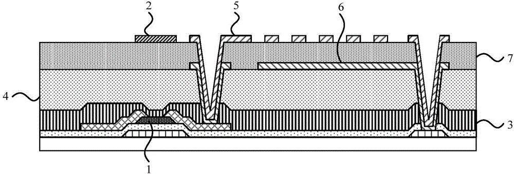
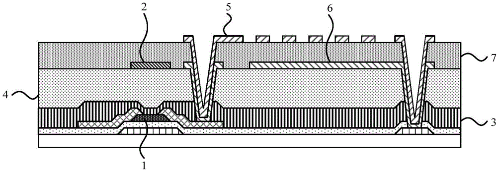
[0093] Such as figure 2 As shown, the display substrate according to one embodiment of the present invention includes:

[0094] A thin film transistor, wherein an active layer 1 is arranged in the...


PUM


Abstract

The present invention relates to a display substrate and a manufacturing method thereof, and a display apparatus. The display substrate comprises: a thin film transistor which is provided with an active layer therein; and a light shield layer which is arranged over the active layer and is used for shielding lights irradiating towards the active layer. According to the technical scheme of the present invention, the light shield layer is arranged over the active layer, so that external lights can be effectively prevented from irradiating to the active layer in the thin film transistor, thereby avoiding unstable performance of the thin film transistor caused by influence on the active layer from the outside illumination.

Description

technical field [0001] The present invention relates to the field of display technology, in particular, to a display substrate, a display device and a method for manufacturing a display substrate. Background technique [0002] IGZO is an oxide containing indium, gallium and zinc. The carrier mobility is 20 to 30 times that of amorphous silicon. It is used to make the active layer of TFT (thin film transistor) can greatly improve the TFT to the pixel electrode. The charge and discharge rate improves the response speed of the pixel and achieves a faster refresh rate. At the same time, the faster response also greatly improves the row scanning rate of the pixel, making ultra-high resolution possible in TFT-LCD. In addition, IGZO displays have higher energy efficiency levels and are more efficient due to the reduced number of transistors and increased light transmittance per pixel. [0003] However, when IGZO is used to make the active layer in a thin film transistor, because I...

Claims


Application Information

Patent Timeline
IPC IPC(8): H01L27/12H01L21/77G02F1/136
Inventor 崔承镇金宰弘
Owner BOE TECH GRP CO LTD
Learn More