Voltage surge protection device and manufacturing method thereof

A technology for protecting devices and voltage surges, which is applied in semiconductor/solid-state device manufacturing, electric solid-state devices, electrical components, etc. fast flow effect

Active Publication Date: 2019-01-11
BEIJING YANDONG MICROELECTRONICS +1
View PDF7 Cites 0 Cited by
  • Summary
  • Abstract
  • Description
  • Claims
  • Application Information

AI Technical Summary

Problems solved by technology

However, the existing semiconductor surge protection devices have the following shortcomings: only one-way surge protection capability, even if there is bidirectional protection capability, the forward and reverse protection capabilities are unbalanced, and the protection response speed is slow, etc.

Method used


Image

  • Voltage surge protection device and manufacturing method thereof
  • Voltage surge protection device and manufacturing method thereof
  • Voltage surge protection device and manufacturing method thereof

Examples


Embodiment 1

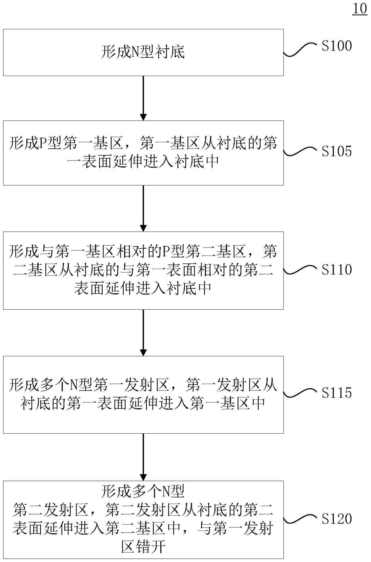
[0051] figure 1 It is the flow process of manufacturing the voltage surge protection device of this embodiment Figure 10 . The following combination figure 1 The flow chart and the corresponding structural views are used to explain the present invention in detail.

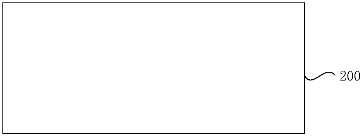
[0052] Step S100, forming an N-type substrate 200, such as figure 2 shown.

[0053]Preferably, the thickness of the substrate 200 used in the present invention is 65%-95% of the substrate thickness of existing voltage surge protection devices. For example, the thickness of the existing substrate is usually 200-230 microns, while the thickness of the substrate of the present invention is about 150-190 microns. Using such a thin substrate, through process adjustment, under the premise of achieving the surge protection capability, the push-in time of the deep junction P++ implanted region described later can be shortened, and the volume of the device can be reduced at the same time.

[0054] S105 , forming a P...

Embodiment 2

[0095] Embodiment 2 is similar to the method and device structure formed in Embodiment 1, except that the conductivity type N in Embodiment 1 is changed to P, and P is changed to N. Therefore, no further details are given here.

[0096] Figure 11 It is an application diagram of the surge protection device according to the present invention, which has two protection units, forward and reverse, to discharge the forward and reverse surges in the line, so as to protect the safe and stable operation of the system connected in parallel with it .


PUM


Abstract

The invention discloses a voltage surge protection device and a manufacturing method thereof. The voltage surge protection device includes a substrate of a first conductivity type, a first base area of a second conductivity type which extends into the substrate from the first surface of the substrate, a second base area of the second conductivity type which is opposite to the first base area and extends into the substrate from the second surface of the substrate which is opposite to the first surface, a plurality of first emission areas of the first conductivity type which extend into the first base area from the first surface of the substrate, and a plurality of second emission areas of a first conductivity type which extend into the second base area from the second surface of the substrate, wherein the first emission areas and the second emission areas are arranged in a staggered manner, and the first conductivity type and the second conductivity type are complementary. The voltage surge protection device provided by the invention can provide forward and reverse surge protection. The voltage surge protection device has the advantages of balanced forward and reverse surge protection abilities, high current discharge speed and small size.

Description

technical field [0001] The invention relates to the technical field of semiconductors, in particular to a voltage surge protection device and a manufacturing method thereof. Background technique [0002] With the rapid development of electronic technology, unexpected voltage transients and surge currents often degrade the performance of the whole system, cause malfunctions or even damage. Especially in communication systems, surges such as lightning strikes, power supply voltage fluctuations, and electromagnetic induction will have a great impact on or even damage communication equipment. [0003] Semiconductor surge protection devices have the superior performance of precise conduction, infinite repetition and fast response, which are far beyond the reach of other instantaneous overvoltage protection devices. However, existing semiconductor surge protection devices have the following shortcomings: only one-way surge protection capability, even if there is bidirectional pro...

Claims


Application Information

Patent Timeline
Patent Type & Authority Patents(China)
IPC IPC(8): H01L27/02H01L27/082H01L29/74H01L29/08H01L29/10H01L21/8222H01L21/332
Inventor 杨显精张守明淮永进刘伟唐晓琦杨京花李洪朋路和超
Owner BEIJING YANDONG MICROELECTRONICS
Why Eureka
Try Eureka