Wiring structure for GOA (Gate driver On Array) circuit
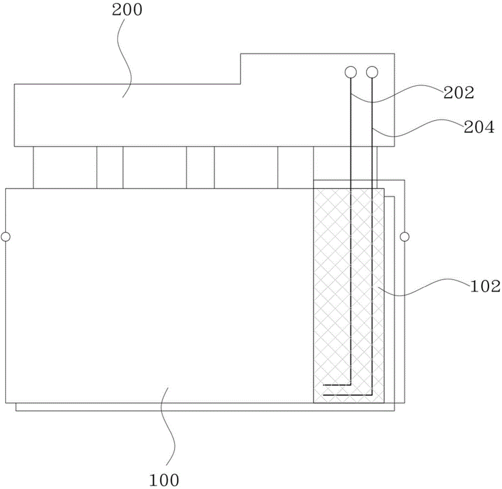
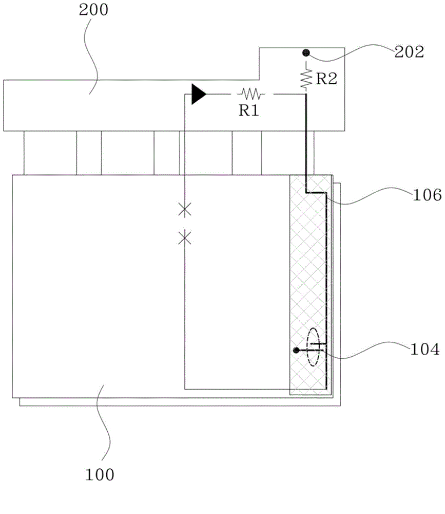
A technology of array substrate row and line structure, applied to instruments, static indicators, etc., can solve the problems of high-frequency signal interference, affecting GOA circuit signal transmission, etc., and achieve the goal of reducing high-frequency signal interference, simplifying circuit design, and reducing the number Effect
- Summary
- Abstract
- Description
- Claims
- Application Information
AI Technical Summary
Problems solved by technology
Method used
Image
Examples
Embodiment Construction
[0024] In order to make the technical content disclosed in this application more detailed and complete, reference may be made to the drawings and the following various specific embodiments of the present invention, and the same symbols in the drawings represent the same or similar components. However, those skilled in the art should understand that the examples provided below are not intended to limit the scope of the present invention. In addition, the drawings are only for schematic illustration and are not drawn according to their original scale.
[0025] The specific implementation manners of various aspects of the present invention will be further described in detail below with reference to the accompanying drawings.
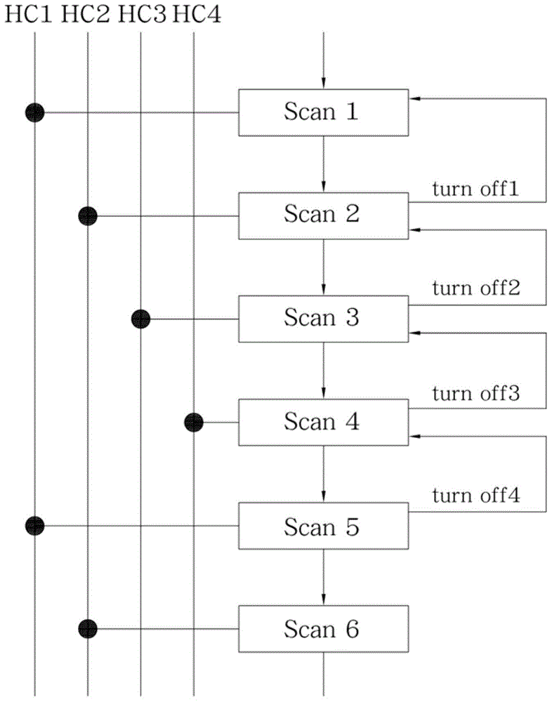
[0026] figure 1 A schematic diagram of a driving principle of a GOA circuit in the prior art is shown. refer to figure 1 , the GOA circuit includes multi-level scanning lines Scan 1, Scan 2,..., Scan6, wherein the high-frequency clock signal HC1 is input...
PUM
 Abstract
Description
Claims
Application Information
 - R&D Engineer
- R&D Manager
- IP Professional
- Industry Leading Data Capabilities
- Powerful AI technology
- Patent DNA Extraction
Browse by: Latest US Patents, China's latest patents, Technical Efficacy Thesaurus, Application Domain, Technology Topic, Popular Technical Reports.
© 2024 PatSnap. All rights reserved.Legal|Privacy policy|Modern Slavery Act Transparency Statement|Sitemap|About US| Contact US: help@patsnap.com


