OLED pixel circuit and its display device
A pixel circuit and electrode technology, which is applied in the field of OLED pixel circuits and display devices, can solve the problems of uneven light emission, uneven light emission of display panels, inconsistent brightness of OLED devices, etc., and achieve the effect of compensation for uneven light emission
- Summary
- Abstract
- Description
- Claims
- Application Information
AI Technical Summary
Problems solved by technology
Method used
Image
Examples
Embodiment 1
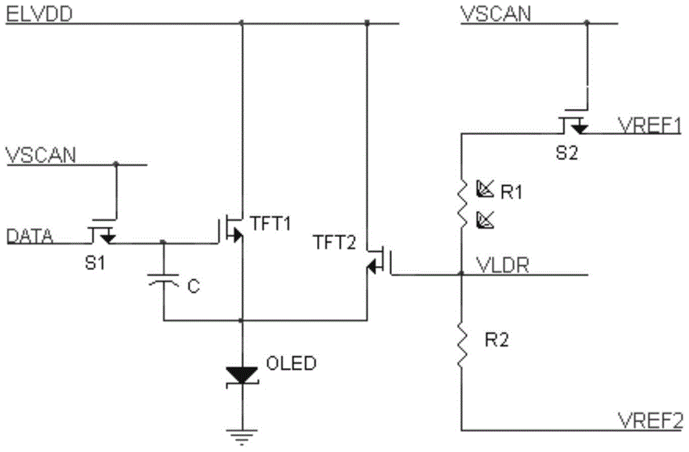
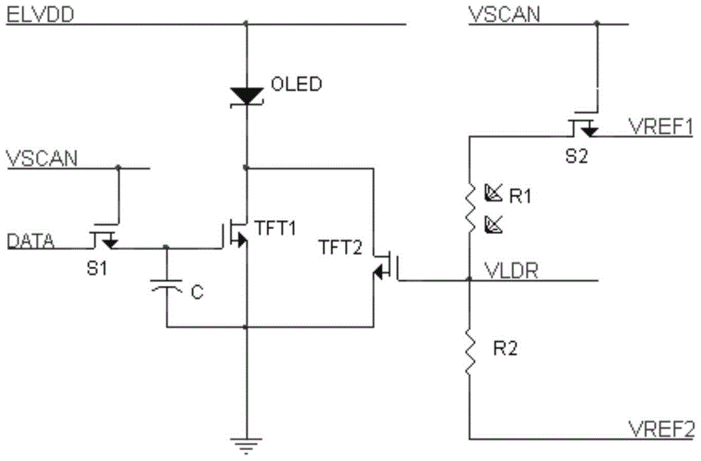
[0045] This embodiment provides an OLED pixel circuit, which uses a positive coefficient photoresistor to compensate the driving circuit of the N-type thin film transistor. The specific circuit structure is as follows: figure 1 , 2 shown.
[0046] In the OLED pixel circuit, the sensing element is a photoresistor, and the compensation unit also includes a synchronous transistor, a compensation drive tube and a voltage dividing resistor, wherein:
[0047] The photoresistor and the voltage dividing resistor are connected in series to form a series branch, the first end of the series branch is a constraint end and is connected to the synchronous transistor, and the second end is a free end and is connected to the second reference voltage end. figure 1 Among them, one end of the photoresistor R1 in the series branch is a constraint end and is connected to the first pole of the synchronous transistor S2, and one end of the voltage dividing resistor R2 in the series branch is a free...
Embodiment 2
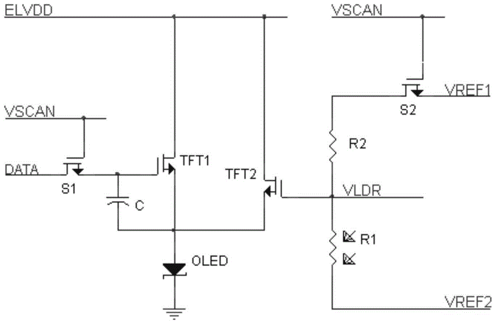
[0064] This embodiment provides an OLED pixel circuit, which uses a negative coefficient photoresistor to compensate the driving circuit of the N-type thin film transistor. The specific circuit structure is as follows: image 3 , 4 shown.
[0065] In the OLED pixel circuit, the synchronous transistor S2 and the compensating driving tube TFT2 are N-type thin film transistors, and the photosensitive resistor R1 is a negative coefficient photosensitive resistor whose resistance value decreases with the enhancement of the OLED brightness, and the free end of the series branch is the photosensitive resistor R1 One end of the voltage dividing resistor R2 is not connected. For negative coefficient photoresistors, the resistance value shows a large resistance value under the condition of no light; under the condition of light, the resistance value becomes smaller and the resistance value becomes smaller as the light increases.
[0066] image 3 Shown is a structure in which N-type ...
Embodiment 3
[0076] This embodiment provides an OLED pixel circuit, which uses a positive coefficient photoresistor to compensate the driving circuit of the P-type thin film transistor. The specific circuit structure is as follows: Figure 5 , 6 shown.
[0077] In the OLED pixel circuit, the synchronous transistor S2 and the compensating driving tube TFT2 are P-type thin film transistors, the photoresistor R1 is a positive-coefficient photoresistor whose resistance value increases with the brightness of the OLED, and the free end of the series branch is the photoresistor R1 One end of the voltage dividing resistor R2 is not connected.
[0078] Figure 5Shown is a structure in which a P-type thin film transistor is used in the OLED pixel circuit, and the compensation unit uses a positive coefficient photoresistor R1 to measure light on the OLED; in the drive unit, the first pole of the output transistor TFT1 is connected to the first input voltage terminal and the storage capacitor The s...
PUM
 Abstract
Description
Claims
Application Information
 - R&D
- Intellectual Property
- Life Sciences
- Materials
- Tech Scout
- Unparalleled Data Quality
- Higher Quality Content
- 60% Fewer Hallucinations
Browse by: Latest US Patents, China's latest patents, Technical Efficacy Thesaurus, Application Domain, Technology Topic, Popular Technical Reports.
© 2025 PatSnap. All rights reserved.Legal|Privacy policy|Modern Slavery Act Transparency Statement|Sitemap|About US| Contact US: help@patsnap.com


