Touch panel array

A touch panel and array technology, applied in the field of microelectronics, can solve the problems of having to open a hole on the front to make a physical HOME button, limiting the effective display area of ​​a mobile phone, and unable to achieve substantial improvement, so as to achieve miniaturization and improve fingerprints. Recognition accuracy, easy-to-achieve effects

Active Publication Date: 2015-08-12
叶志 +2
View PDF5 Cites 7 Cited by
  • Summary
  • Abstract
  • Description
  • Claims
  • Application Information

AI Technical Summary

Problems solved by technology

One is to match the front fingerprint recognition, even if it will damage the appearance of the mobile phone, but it has to be a physical HOME button on the front, which makes the mobile phone ID design difficult; the second is to use a new IFS solution similar to Goodix to integrate the fingerprint recognition sensor Doing it under the cover glass of the mobile phone is actually not much different from opening a hole in this way, but it can be connected with the glass screen and cannot achieve substantial improvement
Whether it is IFS or a physical HOME button, opaque physical buttons can only occupy an additional area of ​​the entire phone panel, limiting the effective display area of ​​the phone
Such defects are obviously incompatible with today's trend of large-screen smartphones
Especially for wearable devices that are about to be popularized, such as smart watches, the experience and security of mobile payment on smart watches will be affected due to the inability to place non-transparent fingerprint recognition modules

Method used


Image

  • Touch panel array
  • Touch panel array
  • Touch panel array

Examples


Embodiment 1

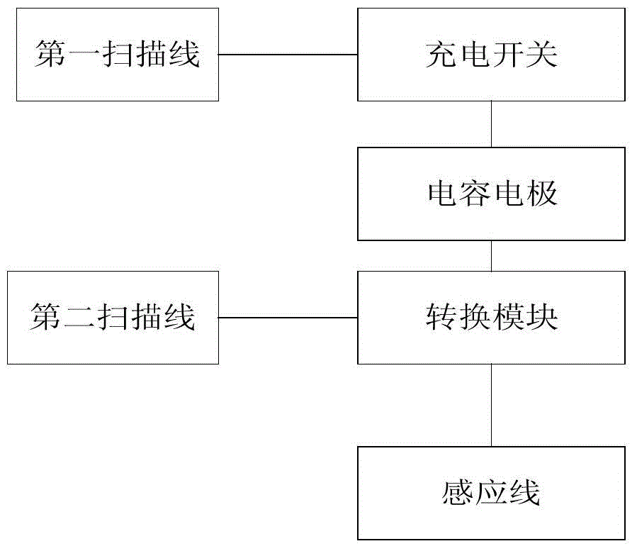
[0045] A touch panel array, including a fingerprint identification area supporting fingerprint identification mode and touch mode. The touch panel array is composed of several array elements arranged in a two-dimensional matrix, and the array elements in this embodiment are enclosed areas surrounded by any two adjacent scanning lines and any two adjacent sensing lines.

[0046] In this embodiment, each array element in the fingerprint identification area corresponds to the first scan line with the earlier timing and the second scan line with the later timing, as shown in figure 1 As shown, each array element includes:

[0047] Capacitive electrodes (in this embodiment, self-capacitance electrodes) are used to form inductive capacitance at the fingerprint contact;

[0048] A charging switch, one end is connected to the capacitor electrode, and the other end is connected to the first scanning line corresponding to the array element, and the charging switch is turned on when a h...

Embodiment 2

[0071] It is the same as Embodiment 1, except that the conversion module has a two-stage amplification function.

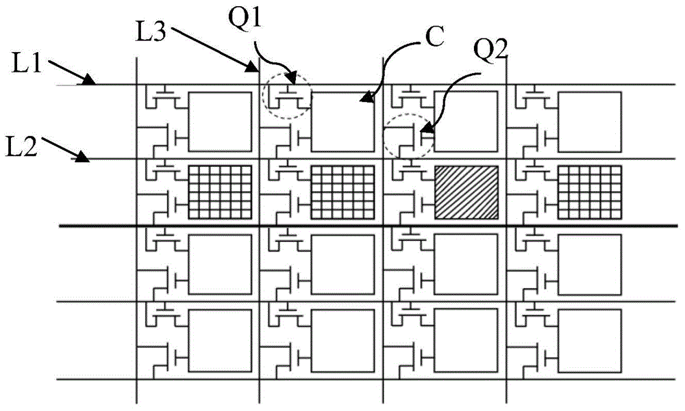
[0072] like Figure 5 As shown, the conversion module of this embodiment includes a third thin film transistor Q3 and a fourth thin film transistor Q4; The source of the thin film transistor Q4 is used as an input terminal and connected to the corresponding second scanning line L2 for voltage sampling, and the drain is used as an output terminal and connected to the corresponding sensing line L3 to output the induced current;

[0073] In this embodiment, each array element is correspondingly provided with a ground line L4, wherein the drain of the third thin film transistor Q3 is connected to the ground line L4, and the source is connected to the gate of the fourth thin film transistor Q4, and the source of the third thin film transistor Q3 is connected to the ground line L4. The terminal is connected to the source of the fourth thin film transistor Q4 through a ...


PUM


Abstract

The invention discloses a touch panel array. Each array element in the fingerprint identification region is correspondingly provided with a first scanning line in a prior time sequence and a second scanning line in a posterior time sequence; each array element comprises a capacitive electrode, a charging switch and a conversion module, wherein each capacitive electrode is used for forming an inductive capacitance at a fingerprint contact part; one end of each charging switch is connected with the corresponding capacitive electrode, and the other end of the charging switch is connected with the first scanning line corresponding to each array element; each charging switch is electrified when a high level is applied to the corresponding first scanning line; the input end of each conversion module is connected with the second scanning line corresponding to each array element and is used for carrying out voltage sampling, and the output end of each conversion module is connected with an induction line corresponding to each array element and used for outputting an inductive current subjected to conversion and amplification; the control end of each conversion module is connected with an inductive electrode and is used for acquiring a voltage control signal. An amplifying effect on the inductive current is realized by arranging the conversion module in each array element of the touch panel array, so that the accuracy of a touch panel is greatly improved; in addition, the touch panel array disclosed by the invention is low in cost and easy to realize.

Description

technical field [0001] The invention relates to the technical field of microelectronics, in particular to a touch panel array. Background technique [0002] Fingerprint identification technology corresponds a person with his fingerprint, and his real identity can be verified by comparing his fingerprint with the pre-saved fingerprint. The skin texture of each person (including fingerprints) varies in pattern, breakpoints and intersections, that is to say, is unique and remains unchanged throughout life. According to the uniqueness and stability characteristics of human fingerprints, identity identification is realized by collecting the fingerprint patterns of the person to be tested, extracting feature information, and comparing with pre-stored fingerprint sample data. Digital fingerprint identification is a high-tech that integrates biotechnology, sensor technology, digital image processing, pattern matching, and other electronic technologies. With the development of soci...

Claims


Application Information

Patent Timeline
Patent Type & Authority Applications(China)
IPC IPC(8): G06F3/044G06F21/32
Inventor 叶志元永刚刘旸
Owner 叶志
Why Eureka
Try Eureka