Touch display panel and driving method thereof

A touch display panel and touch display technology, which is applied in the direction of instruments, computing, and electrical digital data processing, etc., can solve the problem of large public signal delay, increased time for the touch electrode unit to return to the common potential, uneven black screen display, etc. problem, achieve the effect of reducing the delay and reducing the equivalent resistance

Active Publication Date: 2015-08-05
SHANGHAI AVIC OPTOELECTRONICS +1
View PDF3 Cites 18 Cited by
  • Summary
  • Abstract
  • Description
  • Claims
  • Application Information

AI Technical Summary

Problems solved by technology

In order to increase the aperture ratio of the pixel unit, the touch electrode leads are usually arranged under the black matrix between adjacent pixel units, the width of the black matrix is ​​very small, so the width of the touch electrode leads is also very small, and then The resistance of the touch electrode leads is relatively large, especially the touch electrode leads connected to the touch electrode units far away from the touch display circuit, the length of which is too large, resulting in excessive resistance
In the display stage, the large resistance of the touch electrode leads may cause the delay of the common signal loaded on the touch electrode unit to be too large. When other traces couple to the touch electrode unit, the touch electrode unit returns to the common potential. As the time increases, it is easy to cause problems such as flickering, uneven black screen display, and afterimage

Method used


Image

  • Touch display panel and driving method thereof
  • Touch display panel and driving method thereof
  • Touch display panel and driving method thereof

Examples


Embodiment Construction

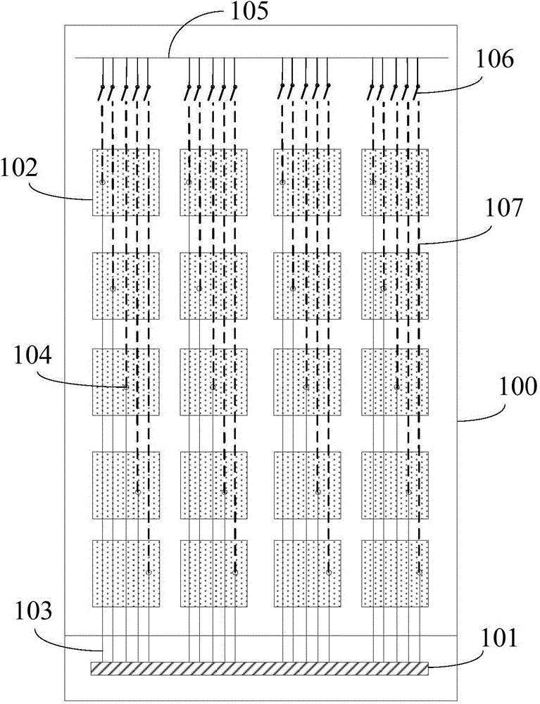
[0022] As mentioned in the background technology, in the prior art in cell TP, the resistance of the touch electrode leads is relatively large, especially the touch electrode leads connected to touch electrode units far away from the touch display circuit, the length of which is too large to cause resistance is too big. In the display stage, the large resistance of the touch electrode leads may cause the delay of the common signal loaded on the touch electrode unit to be too large. When other traces couple to the touch electrode unit, the touch electrode unit returns to the common potential. As the time increases, it is easy to cause problems such as flickering, uneven black screen display, and afterimage.

[0023] In order to solve the above technical problems, the present invention provides a touch display panel, comprising:

[0024] first substrate;

[0025] The electrode array is arranged on the first substrate, the electrode array includes a plurality of electrode units...


PUM


Abstract

The invention discloses a touch display panel and a driving method thereof. The touch display panel comprises a first substrate, wherein a plurality of electrode units, a plurality of switching devices, a touch display circuit and a public lead are arranged on the first substrate; the public lead is used for loading a public signal; each electrode unit is electrically connected with the touch display circuit through a first lead respectively; each electrode unit is electrically connected with the public lead through second leads; each switching device is arranged between each second lead and the public lead in order to switch off the electrical connection between the public lead and the second leads at a touch sensing stage, and connect the public lead and the second leads at a display stage. Thus, each electrode unit loads the public signal through the first leads and the second leads which are connected in parallel at the display stage, so that the equivalent resistance between the electrode units and the touch display circuit at the display stage is reduced, and the delay of the public signal on a touch electrode unit is reduced.

Description

technical field [0001] The present invention relates to the field of display technology, in particular to a touch display panel and a driving method thereof. Background technique [0002] As an input medium, the touch screen is currently the simplest, most convenient and natural way of human-computer interaction. Integrating a touch function on a liquid crystal display (liquid crystal display, LCD) or an organic light-emitting diode (Organic Light-Emitting Diode, OLED) display has become a research and development focus of more and more flat panel display manufacturers. [0003] In order to further reduce the volume of the touch screen and reduce the size of the mobile terminal equipped with the touch screen, in recent years, the display field has developed an in-cell touch display panel (in cell TP), which integrates touch electrodes into a liquid crystal cell Therefore, the size of the touch screen using the in-box touch display technology can be smaller than that using t...

Claims


Application Information

Patent Timeline
Patent Type & Authority Applications(China)
IPC IPC(8): G06F3/041G06F3/044G02F1/1333
CPCG06F3/04164G06F3/04166G06F3/0443G06F3/044
Inventor 金慧俊
Owner SHANGHAI AVIC OPTOELECTRONICS
Why Eureka
Try Eureka