Semiconductor assembly and method of manufacturing the same
一种制作方法、半导体的技术,应用在半导体器件、半导体/固态器件制造、半导体/固态器件零部件等方向,能够解决芯片I/O垫间靠近等问题
- Summary
- Abstract
- Description
- Claims
- Application Information
AI Technical Summary
Problems solved by technology
Method used
Image
Examples
Embodiment 1
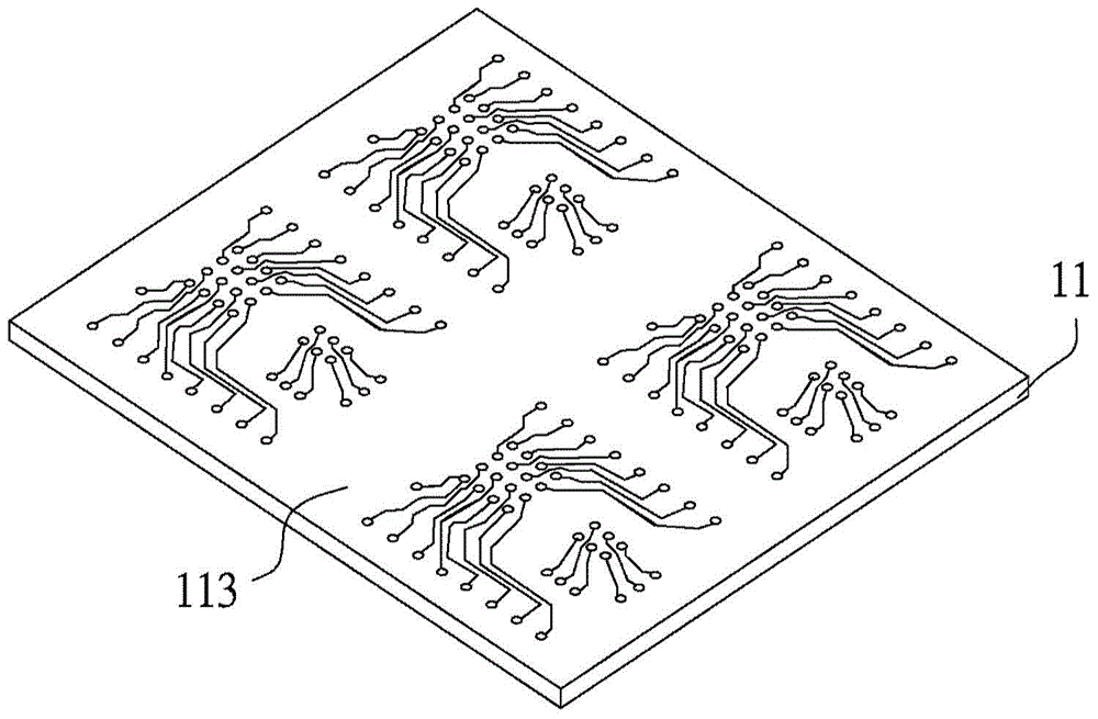
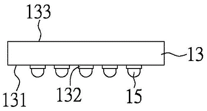
[0074] Figure 1-17 In one implementation aspect of the present invention, a method for manufacturing a semiconductor device includes an interposer, a plurality of semiconductor elements, a base carrier, and a build-up circuit.
[0075] like Figure 17 As shown, the semiconductor assembly 100 includes an interposer 11', a semiconductor device 13, a substrate carrier 20, and a build-up circuit 301. The interposer 11' and the semiconductor device 13 are attached to the base carrier 20 using the adhesive 191, and the semiconductor device 13 is placed in the through opening 205 of the base carrier 20. The build-up circuit 301 covers the interposer 11' and the base carrier 20 from below, and is electrically coupled to the first contact pad 112 of the interposer 11' through the first conductive blind hole 317.
[0076] figure 1 , 3 , 4, 6, and 8 are cross-sectional views of the chip-interposer stacking subassembly process in an implementation aspect of the present invention, f...
Embodiment 2
[0091] Figure 18-23 A method diagram of another semiconductor assembly according to another embodiment of the present invention, wherein the semiconductor assembly has a spacer used in the interposer attaching step, and a cover plate used for heat dissipation of the semiconductor element.
[0092] For the purpose of brief description, any statement in the above-mentioned embodiment 1 that can be used for the same application is incorporated here, and there is no need to repeat the same statement.
[0093] Figure 18 is a cross-sectional view of the substrate carrier 20 , which has a positioning member 217 and a through opening 205 . The positioning member 217 can be formed by removing a selected portion of the metal plate 21 , or by depositing a pattern of metal material or plastic material on the first surface 201 of the metal plate 21 . The positioning member 217 is usually made by electroplating, etching, or mechanical cutting. Accordingly, the positioning member 217 ex...
Embodiment 3
[0101] Figure 24-32 A method diagram illustrating yet another semiconductor device according to another embodiment of the present invention, the semiconductor device includes additional build-up circuitry thermally connected to the semiconductor device and electrically coupled to the substrate carrier.
[0102] For the purpose of brief description, any statements in the above embodiments that can be used in the same way are incorporated here, and there is no need to repeat the same statements.
[0103] Figure 24 is a cross-sectional view of the substrate carrier 20 , which has a through opening 205 and a positioning member 247 . In this figure, the base carrier 20 has a conductive layer 24 on the sidewalls of the through opening 205 and on opposite surfaces of the dielectric layer 23 with a thickness of 0.5 mm. The positioning member 247 can be formed on the underlying conductive layer 24 by pattern deposition, wherein the pattern deposition methods include electroplating,...
PUM
 Abstract
Description
Claims
Application Information
 - R&D Engineer
- R&D Manager
- IP Professional
- Industry Leading Data Capabilities
- Powerful AI technology
- Patent DNA Extraction
Browse by: Latest US Patents, China's latest patents, Technical Efficacy Thesaurus, Application Domain, Technology Topic, Popular Technical Reports.
© 2024 PatSnap. All rights reserved.Legal|Privacy policy|Modern Slavery Act Transparency Statement|Sitemap|About US| Contact US: help@patsnap.com


