
Method for using graphene to determining copper substrate surface crystal orientation

A technology of copper substrate and graphene, which is applied in the direction of analyzing materials through chemical reactions, can solve the problems of high cost and complicated judgment steps, and achieve the effect of low cost and high repeatability

Active Publication Date: 2015-07-29
SHANGHAI INST OF MICROSYSTEM & INFORMATION TECH CHINESE ACAD OF SCI
View PDF5 Cites 5 Cited by
  • Summary
  • Abstract
  • Description
  • Claims
  • Application Information

AI Technical Summary

Problems solved by technology

[0006] In view of the above-mentioned shortcoming of prior art, the purpose of the present invention is to provide a kind of method that utilizes graphene to judge copper substrate surface crystal orientation, is used to solve the complex step of judging copper substrate surface crystal orientation in the prior art, cost Expensive and other issues

Method used


Image

  • Method for using graphene to determining copper substrate surface crystal orientation
  • Method for using graphene to determining copper substrate surface crystal orientation
  • Method for using graphene to determining copper substrate surface crystal orientation

Examples


Embodiment 1

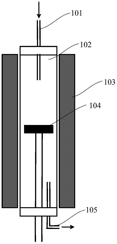
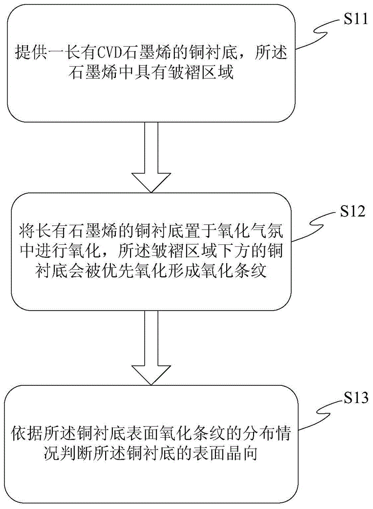
[0034] Such as Figure 1 ~ Figure 2 As shown, the present embodiment provides a method for determining the crystal orientation of a copper substrate surface using graphene, at least including the following steps:

[0035] Such as figure 2 As shown, step 1) S11 is first performed to provide a copper substrate with CVD graphene, and the graphene has wrinkled regions.

[0036] As an example, the copper substrate is a polycrystalline copper substrate. In addition, the present invention is also applicable to all other polycrystalline metal substrates suitable for growing graphene and capable of being oxidized, such as cobalt and nickel.

[0037] Large-area continuous graphene can be obtained by chemical vapor deposition, but the graphene prepared by this method often has more wrinkled regions.

[0038] As an example, the graphene is a graphene continuous film or a graphene single crystal. And, described graphene continuous film can be monolayer graphene continuous film or mult...

Embodiment 2

[0049] Such as Figure 1 ~ Figure 2 As shown, this embodiment provides a method for determining the crystal orientation of a copper substrate surface using graphene, wherein the graphene is a graphene single crystal, oxidized by air, and oxidized at normal pressure and at a temperature of 200° C. for 30 minutes .

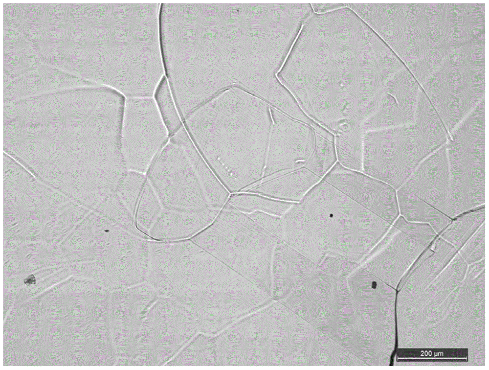
[0050] Figure 5 and Figure 6 Respectively, the copper substrate with graphene is treated by the present embodiment before and after the light microscope. Compared Figure 5 and Figure 6 It can be clearly found that after the treatment of this embodiment, the color of the copper surface without the graphene single crystal protection area has changed significantly, indicating that the copper surface in these areas is severely oxidized, while the color of the area protected by the graphene single crystal There is no significant change, indicating that graphene has a better anti-oxidation protection ability for copper. In addition, darker oxidation stripes appe...


PUM


Abstract

The present invention provides a method for using graphene to determining copper substrate surface crystal orientation. The method at least comprises: 1) providing a copper substrate with growing chemical vapor deposition (CVD) graphene, wherein the wrinkle region exists in the graphene; 2) placing the obtained copper substrate in an oxidizing atmosphere to oxidize, wherein the copper substrate positioned below the wrinkle region is preferentially oxidized to form oxidation stripes; and 3) according to the distribution condition of the oxidation stripes on the copper substrate surface, judging the copper substrate surface crystal orientation. According to the present invention, the determination method has characteristics of high repeatability, simpleness, easy performing, and low cost. With the method of the present invention, the surface crystal orientation distribution condition of the polycrystalline copper substrate with the graphene growing through the chemical vapor deposition can be easily known.

Description

technical field [0001] The invention belongs to the field of metal substrate characterization, in particular to a method for determining the crystal orientation of a copper substrate surface by using graphene. Background technique [0002] Since two Russian-born scientists Andre Geim and Konstantin Novoselov published the first paper on graphene in 2004, graphene has stirred up huge waves in the scientific community, and its appearance is expected to trigger a new era in the field of modern electronic technology. revolution. Graphene is a planar film composed of carbon atoms with sp2 hybrid orbitals forming a hexagonal honeycomb lattice, a two-dimensional material with a thickness of only one carbon atom. Graphene is currently the thinnest but also the hardest nanomaterial in the world. It has the advantages of high light transmittance, high electron mobility, high current density, high mechanical strength, and easy modification. In addition, because of its extremely low r...

Claims


Application Information

Patent Timeline
IPC IPC(8): G01N21/75
Inventor 张燕辉于广辉陈志蓥王斌隋妍萍张浩然张亚欠李晓良
Owner SHANGHAI INST OF MICROSYSTEM & INFORMATION TECH CHINESE ACAD OF SCI
Learn More