Semi-super-junction MOSFET structure and manufacturing method thereof

A fabrication method and semi-superjunction technology, applied in semiconductor/solid-state device manufacturing, semiconductor devices, electrical components, etc., can solve problems such as process capability limitations, and achieve the goal of expanding application fields, high withstand voltage capability, and increasing withstand voltage range. Effect

Active Publication Date: 2015-07-15
WUXI TONGFANG MICROELECTRONICS
View PDF5 Cites 6 Cited by
  • Summary
  • Abstract
  • Description
  • Claims
  • Application Information

AI Technical Summary

Problems solved by technology

[0010] For super-junction MOSFETs, the withstand voltage is mainly determined by the P-pillars of the deep trench structure, but the limitation of process capability often limits the continued development in the direction of high voltage / ultra-high voltage

Method used


Image

  • Semi-super-junction MOSFET structure and manufacturing method thereof
  • Semi-super-junction MOSFET structure and manufacturing method thereof
  • Semi-super-junction MOSFET structure and manufacturing method thereof

Examples


Embodiment 1

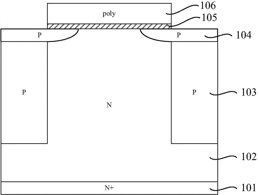
[0076] The present invention provides a semi-superjunction MOSFET structure, please refer to image 3 , shown as a schematic diagram of the structure, comprising at least one transistor cell comprising:

[0077] An N-type heavily doped substrate 201 and an N-type auxiliary layer 202 and an N-type drift layer 203 sequentially formed on the N-type heavily doped substrate 201;

[0078] A first P column 204 and a second P column 205 are formed in the N-type drift layer 203;

[0079] The first P-type body region 206 and the second P-type body region 207 are connected to the tops of the first P-pillar 204 and the second P-pillar 205 respectively, and the first P-type body region 206 and the second P-type body region 207 is located in the N-type drift layer 203;

[0080] A gate structure is formed on the surface of the N-type drift layer 203; the gate structure is located between the first P column 204 and the second P column 205, and both ends of the gate structure are connected t...

Embodiment 2

[0089] The present invention also provides a method for fabricating a semi-superjunction MOSFET structure, comprising the following steps:

[0090] See first Figure 5 , performing step S1: providing a semiconductor substrate sequentially comprising an N-type heavily doped substrate 201 and a first N-type epitaxial layer 215 from bottom to top, and performing P-type impurity implantation on the top of the first N-type epitaxial layer 215 , forming a first pair of P island structures 2101 arranged at intervals. Wherein, the part of the first N-type epitaxial layer 215 below the first pair of P-island structures serves as an N-type auxiliary layer of the semi-superjunction MOSFET.

[0091] then see Figure 6, performing step S2: forming a second N-type epitaxial layer 216 on the surface of the first N-type epitaxial layer 215, and performing P-type impurity implantation in the second N-type epitaxial layer 216 to form a second pair of P island structure 2102 ; the second pair...


PUM


Abstract

The invention provides a semi-super-junction MOSFET structure and a manufacturing method thereof. The structure comprises at least one transistor unit. Each transistor unit comprises an N-type heavily doped substrate, an N-type auxiliary layer and an N-type drift layer, wherein the N-type auxiliary layer and the N-type drift layer are sequentially formed on the N-type heavily doped substrate; a first P column and a second P column are formed in the N-type drift layer; the top ends of the first P column and the second P column are connected with a first P-type area and a second P-type area respectively; a grid structure is formed on the surface of the N-type drift layer and located between the first P column and the second P column; the two ends of the grid structure make contact with the first P-type area and the second P-type area respectively; the bottom ends of the first P column and the second P column are each connected with at least one P-island structure located in the N-type drift layer. Due to existence of the P-island structures, the groove depth can be effectively increased, the doping at the bottom of a groove is optimized, and by combining with a bottom auxiliary depletion layer, under the condition of the existing process capacity, the pressure resistance range of a super-junction MOSFET is further enlarged, and the application fields are extended.

Description

technical field [0001] The invention belongs to the field of semiconductor devices, and relates to a semi-superjunction MOSFET structure and a manufacturing method thereof. Background technique [0002] VDMOSFET (high voltage power MOSFET) can reduce the on-resistance by reducing the thickness of the drain drift region. However, reducing the thickness of the drain drift region will reduce the breakdown voltage of the device. Therefore, in VDMOSFET, the device’s The breakdown voltage and reducing the on-resistance of the device are a pair of contradictions. The super-junction MOSFET adopts a new withstand voltage layer structure, using a series of alternately arranged P-type and N-type semiconductor thin layers. Deplete the P-type and N-type regions to achieve mutual compensation of charges, so that the N-type regions can achieve high breakdown voltage under high doping concentration, thereby obtaining low on-resistance and high breakdown voltage at the same time, breaking th...

Claims


Application Information

Patent Timeline
Patent Type & Authority Applications(China)
IPC IPC(8): H01L29/78H01L21/336H01L29/06
CPCH01L29/0615H01L29/66477H01L29/78
Inventor 白玉明钱振华张海涛
Owner WUXI TONGFANG MICROELECTRONICS
Why Eureka
Try Eureka