Sputtering apparatus

A sputtering device and a predetermined position technology, applied in sputtering plating, ion implantation plating, metal material coating process, etc., can solve the problem of different resistivity of the film layer

Inactive Publication Date: 2015-07-01
BEIJING NAURA MICROELECTRONICS EQUIP CO LTD
View PDF3 Cites 8 Cited by
  • Summary
  • Abstract
  • Description
  • Claims
  • Application Information

AI Technical Summary

Problems solved by technology

[0006] However, when depositing a reactive sputtering film, such as a TiN film, even if the thickness of the film deposited on the substrate is the same everywhere, the resistivity of the film is still different.

Method used


Image

  • Sputtering apparatus
  • Sputtering apparatus
  • Sputtering apparatus

Examples


Embodiment approach

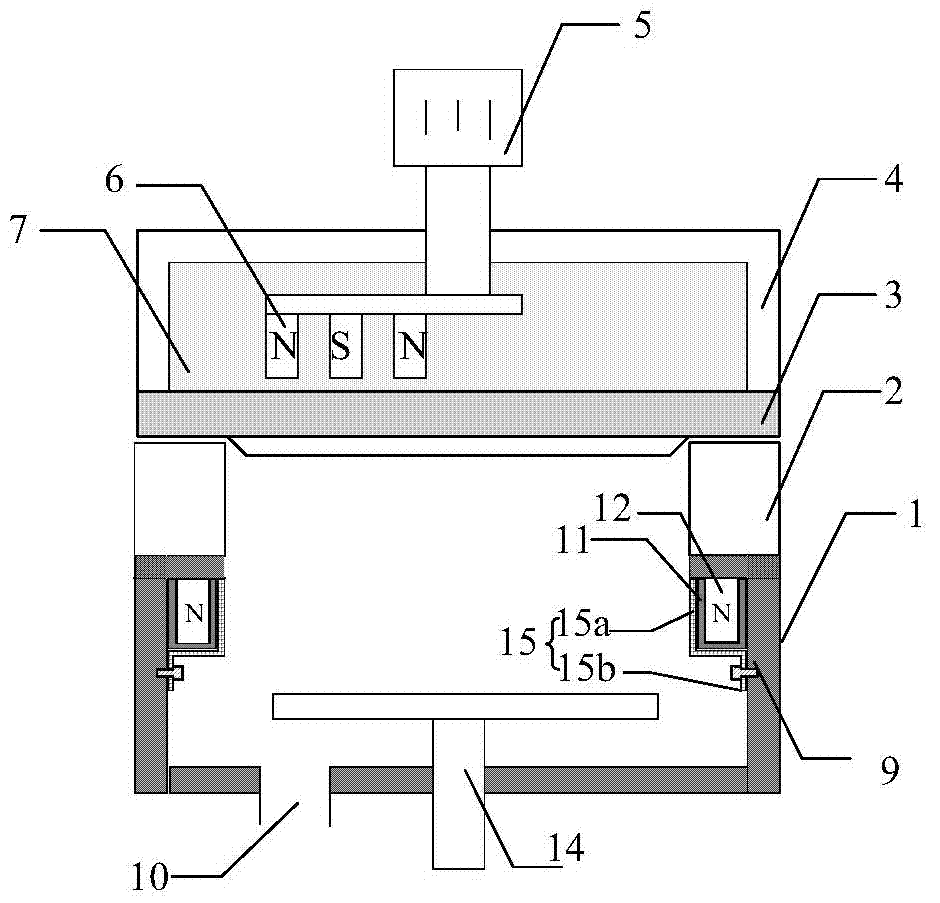
[0042] As the first embodiment of the present invention, such as Figure 4 As shown, the magnetic assembly may include a plurality of magnets 12 and a plurality of housings 15 corresponding to each magnet 12 , and the plurality of housings 15 are disposed around the base 14 . Specifically, a magnet 12 and a spacer 11 covering the magnet 12 are arranged in the accommodation portion 15a of each housing 15, and the mounting portion 15b of each housing 15 is fixed on the inner wall of the process chamber 1 by a fastener 9 superior. In order to evenly distribute the magnetic field strength at the edge of the base 14 , preferably, a plurality of casings 15 are evenly arranged around the base 14 .

[0043] In the sputtering deposition process, the target 3 is bombarded and sputtered, and the sputtered target atoms or molecules move from the surface of the target 3 to the direction of the base 14. At this time, the magnets 12 arranged in the housings 15 The generated magnetic field ...


PUM


Abstract

The invention provides a sputtering apparatus, which comprises a technology chamber, a magnetron and a pedestal for bearing a substrate, the magnetron and the pedestal are arranged in the technology chamber, the magnetron is positioned over the pedestal, wherein the sputtering apparatus also comprises a magnetic element, the magnetic element is arranged at a preset position in the technology chamber for increasing the magnetic field intensity of the preset position; and the preset position is determined according to a material of a target material between the magnetron and the pedestal. When the sputtering apparatus is used for depositing a film layer on the substrate, target material atoms or molecules move by deflecting the preset position, resistivity of the film layer at the preset position is increased, resistivity uniformity of the deposited film layer can be integrally improved, and the film thickness uniformity and the square resistance uniformity of the film layer is improved.

Description

technical field [0001] The present invention relates to the field of semiconductor equipment, in particular to a sputtering device. Background technique [0002] Physical vapor deposition (PVD) generally refers to the film preparation process that uses physical methods to prepare film layers. Physical vapor deposition technology can be applied to many process fields, such as copper interconnection technology and through silicon via (TSV) in the packaging field. ) technology, etc. [0003] Sputtering deposition technology is a typical physical vapor deposition method, figure 1 It is a schematic cross-sectional view of a typical sputtering device. Such as figure 1 As shown, the sputtering device mainly includes: a process chamber 1, a vacuum system 10, a target material 3, a cooling chamber 4 for cooling the target material, a base 14, a magnetron 6, and a motion track for controlling the magnetron 6 The power source 5. During the process, some atoms or molecules of the t...

Claims


Application Information

Patent Timeline
Patent Type & Authority Applications(China)
IPC IPC(8): C23C14/35
Inventor 陈春伟杨玉杰
Owner BEIJING NAURA MICROELECTRONICS EQUIP CO LTD
Why Eureka
Try Eureka