
Top-emission type organic electroluminescent display panel and manufacturing method thereof as well as display device

An electroluminescent display and top-emission technology, which is applied in the direction of circuits, electrical components, and electrical solid devices, can solve problems affecting the display effect of OLED panels, the film thickness of OLED panels, and reduce luminous efficiency, so as to improve luminous efficiency and display effect, reduce the number of film layers, and reduce the effect of process flow

Inactive Publication Date: 2015-06-10
BOE TECH GRP CO LTD
View PDF6 Cites 21 Cited by
  • Summary
  • Abstract
  • Description
  • Claims
  • Application Information

AI Technical Summary

Problems solved by technology

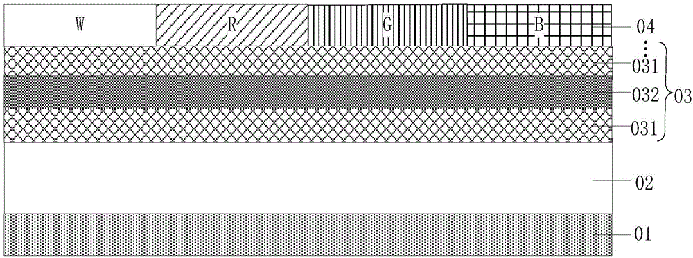
However, the film layer of the OLED panel formed in this way is thicker, the manufacturing process is more complicated, and the light path is increased, the luminous efficiency is reduced, and the display effect of the OLED panel is affected.

Method used


Image

  • Top-emission type organic electroluminescent display panel and manufacturing method thereof as well as display device
  • Top-emission type organic electroluminescent display panel and manufacturing method thereof as well as display device
  • Top-emission type organic electroluminescent display panel and manufacturing method thereof as well as display device

Examples


Embodiment Construction

[0031] The specific implementation manners of the top-emission organic electroluminescent display panel provided by the embodiments of the present invention, its manufacturing method and the display device will be described in detail below with reference to the accompanying drawings.

[0032] Wherein, the thickness and shape of each film layer in the drawings do not reflect the true proportion of the top-emission organic electroluminescent display panel, and the purpose is only to illustrate the content of the present invention.

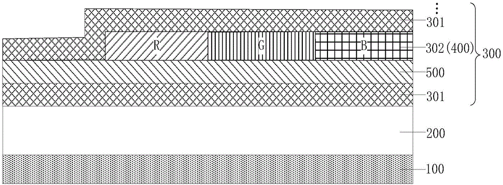
[0033] An embodiment of the present invention provides a top-emission organic electroluminescent display panel, such as Figure 2a to Figure 2d As shown, it includes: a base substrate 100, a white organic light emitting diode 200 and a thin film encapsulation layer 300 sequentially arranged on the base substrate 100; wherein the thin film encapsulation layer 300 includes at least two inorganic thin film layers 301 and at least two layers alternately a...


PUM


Abstract

The invention discloses a top-emission type organic electroluminescent display panel and a manufacturing method thereof as well as a display device. The top-emission type organic electroluminescent display panel comprises a substrate base plate, and a white organic light-emitting diode and a film packaging layer both orderly arranged on the substrate base plate, wherein the film packaging layer comprises at least two film layers and at least one organic film layer, all of which are arranged alternately, wherein one organic film layer is a color filter layer comprising at least three optical filters different in color and capable of realizing all-color display. As one organic film layer in the film packaging layer is the color filter layer, no color filter layer needs to be arranged independently above the film packaging layer, and therefore, the number of the films of the display panel can be reduced, the film structure can be simplified, the process can be shortened and the manufacturing cost can be reduced; in addition, the optical path from the luminous layer to the color filter layer can be shortened, and consequently, the luminous efficiency and the display effect can be improved.

Description

technical field [0001] The invention relates to the field of display technology, in particular to a top-emission organic electroluminescence display panel, a manufacturing method thereof and a display device. Background technique [0002] At present, organic electroluminescent display devices (Organic Electroluminescent Display, OLED) have gradually become the mainstream in the display field due to their excellent performances such as low power consumption, high color saturation, wide viewing angle, thin thickness, and flexibility. OLED can be divided into two types: bottom emission type and top emission type according to the way of light emission. The light emission of bottom emission type OLED comes from the side of the substrate substrate, while the light emission of top emission type OLED comes from the top. [0003] In order to realize the full colorization of large-sized OLED panels, it is generally realized by stacking a top-emitting white organic light emitting diode...

Claims


Application Information

Patent Timeline
Patent Type & Authority Applications(China)
IPC IPC(8): H01L51/52H01L51/56H01L27/32
CPCH10K59/38H10K59/8792H10K59/873H10K50/844H10K50/865H10K71/00
Inventor 李周炫皇甫鲁江朴进山
Owner BOE TECH GRP CO LTD
Learn More