
Display panel and electronic device

一种显示面板、显示区的技术,应用在电数字数据处理、仪器、计算等方向,能够解决可靠性差、静电无法完全被释放、影响盖板贴合效果等问题,达到良好传导作用的效果

Inactive Publication Date: 2015-06-10
SHANGHAI TIANMA MICRO ELECTRONICS CO LTD +1
View PDF9 Cites 52 Cited by
  • Summary
  • Abstract
  • Description
  • Claims
  • Application Information

AI Technical Summary

Problems solved by technology

However, this connection method has poor reliability, and it is difficult to form a good connection between the silver paste and the high-resistance shielding layer, so that static electricity cannot be completely discharged. In addition, the silver paste is also easy to climb to the surface of the upper polarizer, resulting in The surface of the color filter substrate is uneven, which affects the bonding effect of the cover lens

Method used


Image

  • Display panel and electronic device
  • Display panel and electronic device
  • Display panel and electronic device

Examples


Embodiment Construction

[0022] The technical solutions in the embodiments of the present invention will be clearly and completely described below in conjunction with the accompanying drawings in the embodiments of the present invention. Obviously, the described embodiments are only a part of the embodiments of the present invention, rather than all the embodiments. Based on the embodiments of the present invention, all other embodiments obtained by those of ordinary skill in the art without creative work shall fall within the protection scope of the present invention.

[0023] In order to make the above-mentioned objects, features and advantages of the present invention more obvious and understandable, the specific embodiments of the present invention will be described in detail below with reference to the accompanying drawings.

[0024] First, in order for those skilled in the art to better understand the technology of the present invention, the structure of the display panel in the prior art will be intr...


PUM


Abstract

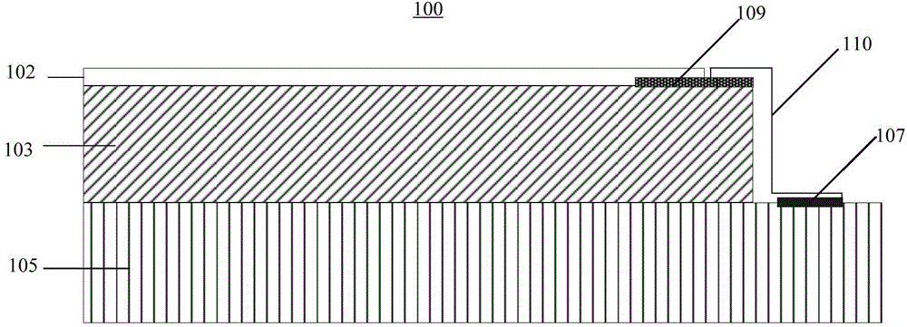
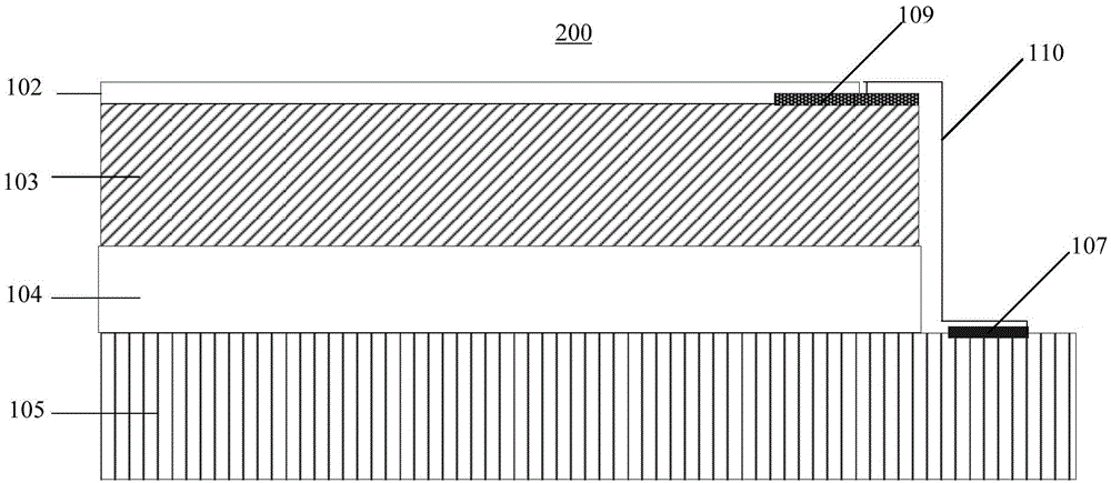
The invention provides a display panel and an electronic device. The display panel comprises a first substrate, a second substrate, a high-resistance shielding layer, a conductive film, a ground welding spot and a conductive connecting portion. The second substrate faces the first substrate. The high-resistance shielding layer is disposed on one side, far away from the second substrate, of the first substrate. The conductive film is disposed between the first substrate and the high-resistance shielding layer. The conductive film comprises a contact portion in contact with the high-resistance shielding layer and an extension portion exposed. The ground welding spot is disposed on one side, close to the first substrate, of the second substrate. The conductive connecting portion electrically connect the extension portion of the conductive film and the ground welding spot The high-resistance shielding layer can be tightly contacted with the conductive film; the conductive film can transfer static electricity of the high-resistance shielding layer to the ground welding spot through the conductive connecting portion, thus good static conduction is achieved, the problem that the static electricity of the high-resistance shielding layer cannot be fully transmitted to the ground welding spot due to poor contact is avoided, and the touch and display performances of the panel is unaffected.

Description

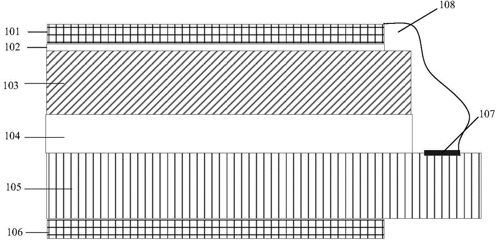
Technical field [0001] The present invention relates to the technical field of liquid crystal displays, in particular to a display panel and electronic equipment. Background technique [0002] The touch liquid crystal display in the prior art generally includes an upper polarizer, a high-resistance shielding layer, a color filter substrate, a liquid crystal layer, an array substrate, and a lower polarizer from top to bottom. The high-resistance shielding layer generally needs to be connected to a GND pad on the array substrate to release static electricity on the high-resistance shielding layer. In the prior art, the high-resistance shielding layer and the grounding solder joint are generally directly connected through silver paste. However, the reliability of this connection method is poor, and it is difficult to form a good connection between the silver paste and the high-resistance shielding layer, so that static electricity cannot be completely discharged. In addition, the s...

Claims


Application Information

Patent Timeline
Patent Type & Authority Applications(China)
IPC IPC(8): G02F1/13G02F1/1333G06F3/041
CPCG02F1/1333G02F1/133308G06F3/041G02F1/133334G06F3/0412G06F2203/04103G06F2203/04107G06F3/0443
Inventor 柴慧平
Owner SHANGHAI TIANMA MICRO ELECTRONICS CO LTD
Learn More