
Vertical NPN device in BCD process and manufacturing method thereof

A vertical type, device technology, applied in semiconductor/solid-state device manufacturing, semiconductor devices, electrical components, etc., can solve problems affecting devices, narrowing of the width of the base region 104, etc., and achieve the effect of reducing process costs

Active Publication Date: 2015-06-03
SHANGHAI HUAHONG GRACE SEMICON MFG CORP
View PDF6 Cites 0 Cited by
  • Summary
  • Abstract
  • Description
  • Claims
  • Application Information

AI Technical Summary

Problems solved by technology

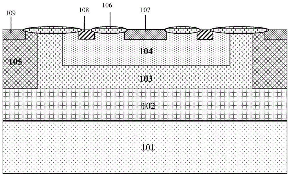
[0004] In the existing BCD process, by further performing N-type light doping on the emitter region 107, that is, N-implantation, to form a graded emitter region (Graded Emitter) to improve the PN junction between the emitter region and the base region of the NPN device, that is, EB The breakdown voltage of the junction, but due to the increase of N-implantation in the emitter region 107, the emitter region 107 will expand to the bottom, which will cause the width of the base region 104 to narrow, which will reduce the gap between the collector region and the emitter region of the device. The punch-through voltage is the CE-punch voltage
When the device is working, CE, that is, the punch-through (Punch) between the collector region and the emitter region may occur before the EB junction is broken down, which affects the device BV

Method used


Image

  • Vertical NPN device in BCD process and manufacturing method thereof
  • Vertical NPN device in BCD process and manufacturing method thereof
  • Vertical NPN device in BCD process and manufacturing method thereof

Examples


Embodiment B

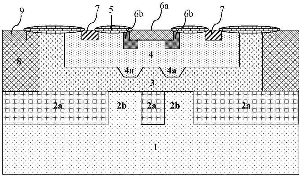
[0035] Such as figure 2 Shown is a schematic structural view of the vertical NPN device in the BCD process of the embodiment of the present invention; the vertical NPN device in the BCD process of the embodiment of the present invention includes:

[0036] The N-type buried layer is formed on the P-type silicon substrate 1, and the N-type buried layer is divided into a buried layer implanted region 2a and a buried layer non-implanted region 2b, and the doping concentration of the buried layer implanted region 2a is higher than that of the buried layer implanted region 2a The doping concentration of the buried layer non-implanted region 2b, the N-type impurity of the buried layer implanted region 2a is formed by N-type ion implantation, the N-type impurity of the buried layer non-implanted region 2b is formed by the buried layer implanted region 2a N-type impurities are formed by lateral diffusion.

[0037] An N-type epitaxial layer 3 is formed on the surface of the N-type bur...


PUM


Abstract

The invention discloses a vertical NPN device in a BCD process. An emitting region consists of a first N+ region and a second N- region, wherein the junction depth of the second N- region is greater than the junction depth of the first N+ region, in addition, the second N- region surrounds the peripheral side of the first N+ region, an embedded layer injection region is not formed right under the second N- region, and the junction depth of a base region positioned right under the second N- region does not expand towards the bottom through the low doping concentration of an embedded layer non-injection region. The invention also discloses a manufacturing method of the vertical NPN device in the BCD process. The second N-region of the device provided by the invention can carry out the transverse exhausting on the base region arranged at the bottom of the first N+ region, so that the BVEBO of the device can be improved. Through the arrangement of the embedded layer non-injection region of the device, the base region arranged right under the second N- region can expand towards the bottom, so that the influence of passing voltage reduction between CEs of the device due to the introduction of the second N- region can be reduced, and meanwhile, greater BVEBO and BVCEO can be obtained at the same time.

Description

technical field [0001] The invention relates to the field of semiconductor integrated circuit manufacturing, in particular to a vertical NPN device in the BCD process; the invention also relates to a method for manufacturing the vertical NPN device in the BCD process. Background technique [0002] The BCD process is a process that can make bipolar transistors (bipolar), CMOS and DMOS devices on the same chip, such as figure 1 Shown is a schematic structural diagram of a vertical NPN device in an existing BCD process; the vertical NPN device in an existing BCD process includes: [0003] A P-type silicon substrate 101 is formed with a highly doped N-type buried layer (NBL) 102 on the silicon substrate 101 . An N-type epitaxial layer is formed on the surface of the N-type buried layer 102, and the collector region 103 is composed of the N-type epitaxial layer. In the N-type epitaxial layer, an N-type sinking layer (NSINK) 105 whose bottom is in contact with the N-type buried ...

Claims


Application Information

Patent Timeline
Patent Type & Authority Applications(China)
IPC IPC(8): H01L29/732H01L29/08H01L29/06H01L21/331
Inventor 钱文生刘冬华吴刚石晶
Owner SHANGHAI HUAHONG GRACE SEMICON MFG CORP
Learn More