
High-speed bridge device for AHB (advanced high-performance bus) accessing on-chip SRAM (static random access memory) and operating method of high-speed bridge device

A working method and bus technology, applied in the direction of memory address/allocation/relocation, instrument, electrical digital data processing, etc., can solve the problem of efficiency reduction and achieve the effect of avoiding the reduction of system continuous reading efficiency

Active Publication Date: 2015-06-03
SHANDONG SINOCHIP SEMICON
View PDF1 Cites 8 Cited by
  • Summary
  • Abstract
  • Description
  • Claims
  • Application Information

AI Technical Summary

Problems solved by technology

The efficiency of the whole system decreases accordingly

Method used


Image

  • High-speed bridge device for AHB (advanced high-performance bus) accessing on-chip SRAM (static random access memory) and operating method of high-speed bridge device
  • High-speed bridge device for AHB (advanced high-performance bus) accessing on-chip SRAM (static random access memory) and operating method of high-speed bridge device
  • High-speed bridge device for AHB (advanced high-performance bus) accessing on-chip SRAM (static random access memory) and operating method of high-speed bridge device

Examples


Embodiment Construction

[0025] The present invention will be further described below in conjunction with the accompanying drawings.

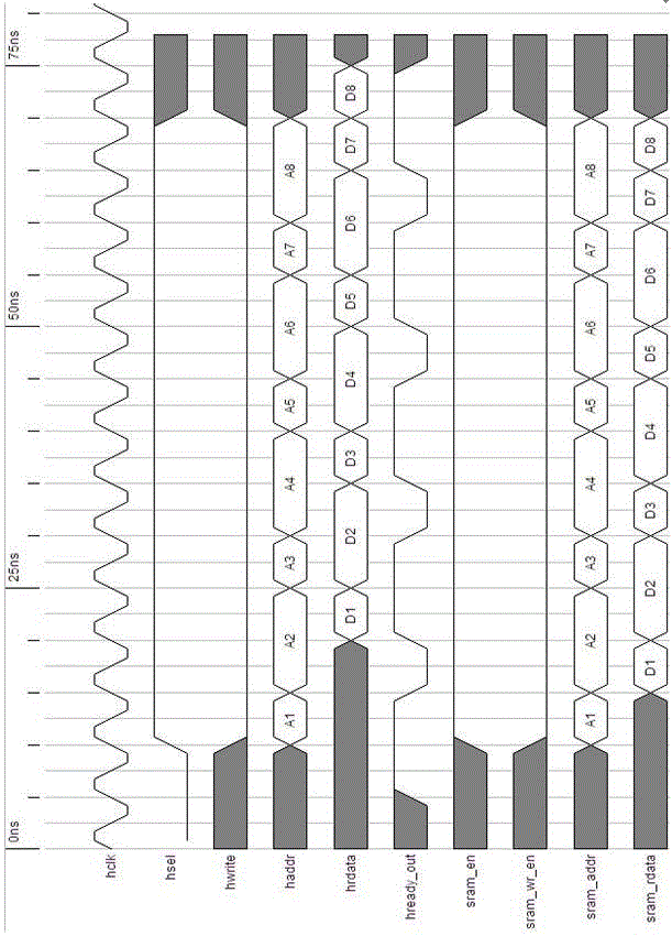
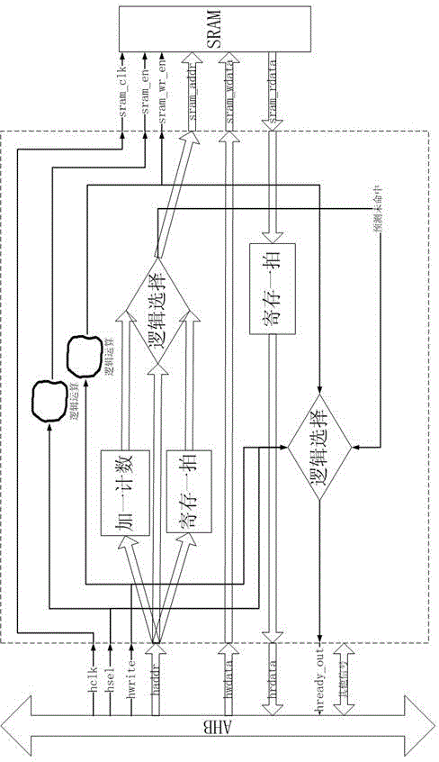
[0026] like image 3 As shown, the present invention adds an address prediction mechanism on the basis of the ordinary AHB to SRAM bridge, compares the bus address and the predicted address, and if they are consistent, the reading can be read in the SRAM one clock cycle in advance, ensuring that the chip meets the timing requirements and the data can be continuous Transmission; the predicted address refers to the address obtained by adding one count. Suppose the address on the current bus is 0x0000_1234. It is the predicted address, and the predicted address is used as the SRAM address when the data of the read operation is returned. Therefore the cost of the present invention is only to increase a 1-up counter and related control logic on the basis of the common bridge, and will not exceed several hundred gates, and the efficiency can be increased by one-third when t...


PUM


Abstract

The invention discloses a high-speed bridge device for an AHB (advanced high-performance bus) accessing an on-chip SRAM (static random access memory), which comprises a register and a plus one counter; during write operation, an SRAM address, i.e. an AHB address of the previous clock cycle, which is obtained after an AHB address is stored by the register for a beat is accessed; during read operation, at the beat of returning read operation data, a predicted address which is obtained after the plus one counter adds one to the AHB address is accessed, and at the beat of incomplete read operation data transmission, the AHB address is the SRAM address, i.e., the current AHB address is accessed. The invention also discloses an operating method of the high-speed bridge device for the AHB accessing the on-chip SRAM. The invention uses the buss bridge with an address prediction mechanism to accelerate the read-write access of the high-capacity SRAM, thus increasing the operating efficiency of the whole system.

Description

technical field [0001] The invention relates to the field of high-speed data processing, in particular to a high-speed bridge device for AHB bus accessing on-chip SRAM and a working method thereof. Background technique [0002] In a system with a high-speed peripheral interface and capable of complex data processing functions, SRAM usually plays the role of data temporary storage. The original intention of using large-capacity SRAM is to improve system efficiency, because in various storage devices, the order of read and write speeds from fast to slow is registers, SRAM, DRAM, FLASH, and traditional hard disks. In the SOC system, the CPU, which is often used in the form of IP, has its own cache to improve efficiency, and there is an interface for operating the cache inside. When other data flow control modules of the system need to cache data, they can choose to mount a large-capacity SRAM on the bus as a cache. The advantage is that it can be used for scheduling by mul...

Claims


Application Information

Patent Timeline
IPC IPC(8): G06F13/16G06F12/02
Inventor 王运哲孙晓宁戴邵新杨萌赵阳刘大铕刘奇浩
Owner SHANDONG SINOCHIP SEMICON
Learn More