


Quick Research
Generate reliable direction feasibility study reports for your R&D in just a few steps.

Technical Q&A
Discover and master advanced knowledge NOW. Basics, ideas, possibilities, all at once.

Find Solutions
As an expert in R&D theories, this can generate solutions to your technical problems instantly.

Evaluate Feasibility
Analyze your overall solution with one click, know your potential R&D risks in advance.

Monitor Landscape
Get weekly tech updates, stay abreast of the latest tech innovations and key insights.
OLED (Organic Light Emitting Diode) display mother board, packaging system and packaging method thereof
A packaging system and packaging method technology, which is applied in the manufacture of electrical components, electrical solid devices, semiconductor/solid devices, etc., can solve the problems of OLED device pollution, UA glue puncture, and entering into the box, so as to achieve simple structure and improve production efficiency , cost-saving effect
- Summary
- Abstract
- Description
- Claims
- Application Information
AI Technical Summary
Problems solved by technology
Method used
Image

Examples
Embodiment 1
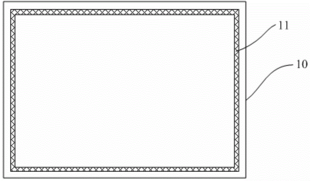
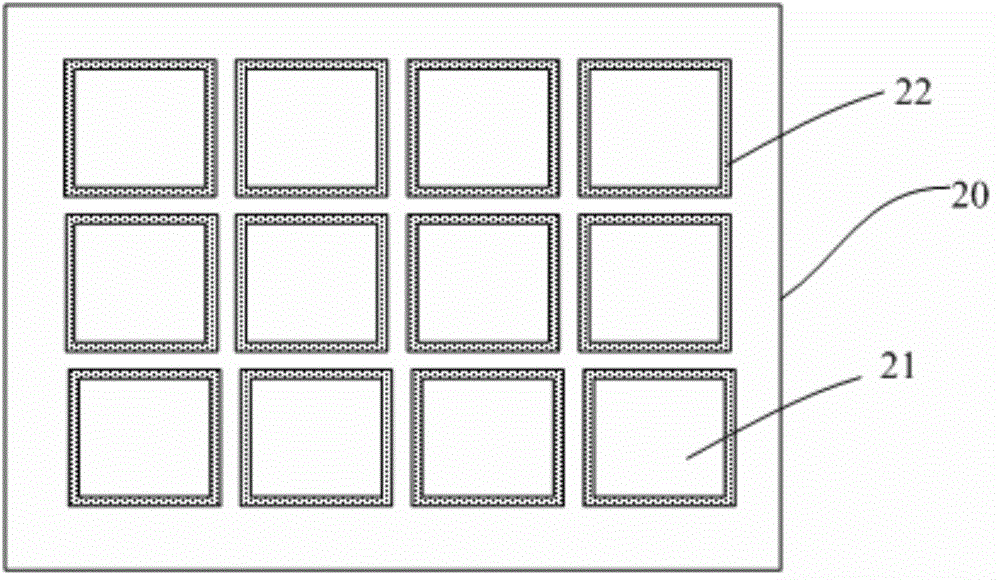
[0050] combine figure 1 and 2 As shown, this embodiment provides an OLED display motherboard, which includes an encapsulation cover 10 and an OLED substrate 20 facing each other, and a sealant is provided between the encapsulation cover 10 and the OLED substrate 20, so that The sealant is arranged on the peripheral area of the OLED display motherboard, and the sealant adopts hot melt adhesive 11 .
[0051]Because in the peripheral area of the OLED display motherboard of this embodiment, the hot melt adhesive 11 is used for sealing between the packaging cover plate 10 and the OLED substrate 20, and the hot melt adhesive 11 itself has better adhesion characteristics than UV adhesives. , the encapsulation cover plate 10 and the OLED substrate 20 can be well sealed, so particles and impurities in the external environment can be effectively prevented from entering the interior of the OLED display motherboard and polluting the devices in the OLED display motherboard, thereby ca...
Embodiment 2
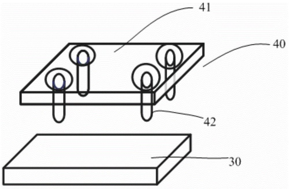
[0056] combine image 3 and 4 As shown, the present embodiment provides a packaging system, including sealant wiring equipment, and the sealant wiring equipment includes: a first carrying machine 30 for carrying the packaging cover 10; a wiring mechanism 40 for hot-melting The glue 11 is routed to the peripheral area of the package cover 10 .
[0057] In this embodiment, the packaging system includes a sealing glue wiring device. By wiring the hot melt glue 11 to the peripheral area of the packaging cover 10 , the sealing is better when the packaging cover 10 and the OLED substrate 20 are aligned.
[0058] Wherein, the wiring mechanism 40 of this embodiment preferably includes a collection unit 43, a tray 41, a plurality of fixed posts 42 arranged on the tray 41, and a driver, the collection unit 43 is used to collect each of the fixed posts 42 and The positional relationship of the reference points on the packaging cover plate 10 to be wired; the driver is used to set e...
Embodiment 3
[0064] This embodiment provides a packaging method for packaging an OLED display motherboard. Wherein, the OLED display motherboard can be the OLED display motherboard described in Embodiment 1, and the packaging method can be applied to the packaging device of Embodiment 2, and the packaging method includes the following steps:
[0065] S01 , use hot melt adhesive 11 to perform wiring on the peripheral area of the package cover 10 .
[0066] This step specifically includes: first placing the packaging cover plate 10 on the first carrying machine 30, determining the positions of the four reference points in the peripheral area of the packaging cover plate 10, and determining the relationship between the four reference points and the hot melt adhesive 11 to be passed. The positional relationship of the wiring area, and use the hot melt adhesive 11 to perform wiring in the peripheral area of the package cover 10; then heat the area where the four reference points of the pa...
PUM
 Abstract
Description
Claims
Application Information
 - R&D Engineer
- R&D Manager
- IP Professional
- Industry Leading Data Capabilities
- Powerful AI technology
- Patent DNA Extraction
Browse by: Latest US Patents, China's latest patents, Technical Efficacy Thesaurus, Application Domain, Technology Topic, Popular Technical Reports.
© 2024 PatSnap. All rights reserved.Legal|Privacy policy|Modern Slavery Act Transparency Statement|Sitemap|About US| Contact US: help@patsnap.com