Silicon heterojunction solar cell structure and manufacturing method thereof

A solar cell and silicon heterojunction technology, which is applied in the manufacture of final products, sustainable manufacturing/processing, circuits, etc., can solve the problems of poor interface contact ability and easy peeling, and achieve the effect of improving the tension of the solder strip

Inactive Publication Date: 2015-05-20
AU OPTRONICS CORP
View PDF0 Cites 1 Cited by
  • Summary
  • Abstract
  • Description
  • Claims
  • Application Information

AI Technical Summary

Problems solved by technology

However, this solar cell structure has at least the following problems in the back electrode part: the interface contact ability between the surface of the single-crystal transparent conductive oxide layer and NiV / Ag is too poor, which leads to peeling (peeling) easily when Ribbon (metal ribbon) is welded and other bad situations, and the tension value of the Ribbon during the tensile test is less than 1N / m 2

Method used


Image

  • Silicon heterojunction solar cell structure and manufacturing method thereof
  • Silicon heterojunction solar cell structure and manufacturing method thereof
  • Silicon heterojunction solar cell structure and manufacturing method thereof

Examples


Embodiment Construction

[0038] In order to make the technical content disclosed in this application more detailed and complete, reference may be made to the drawings and the following various specific embodiments of the present invention, and the same symbols in the drawings represent the same or similar components. However, those skilled in the art should understand that the examples provided below are not intended to limit the scope of the present invention. In addition, the drawings are only for schematic illustration and are not drawn according to their original scale.

[0039] The specific implementation manners of various aspects of the present invention will be further described in detail below with reference to the accompanying drawings.

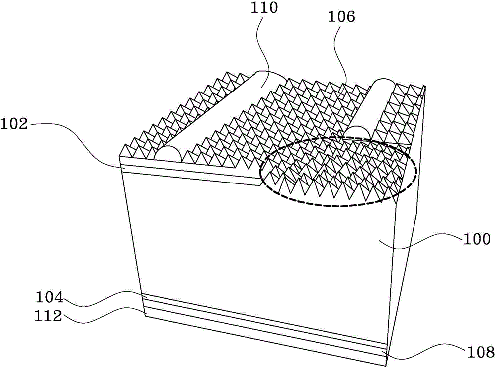
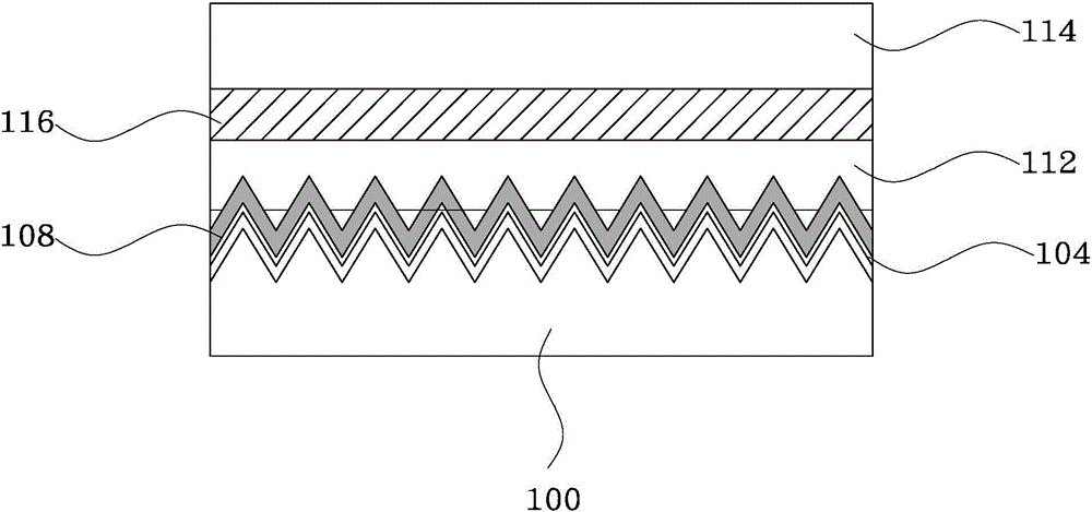
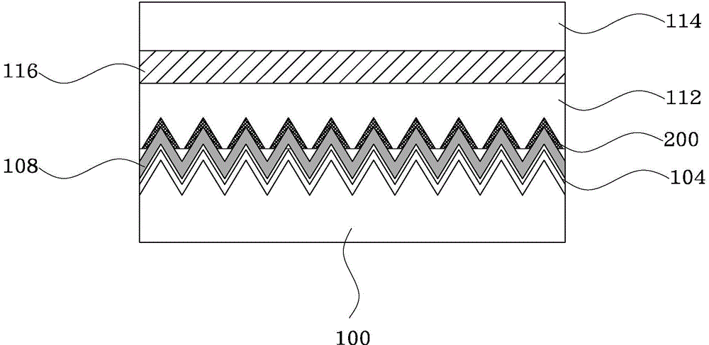
[0040] figure 1 A schematic structural diagram of a silicon heterojunction solar cell in the prior art is shown. figure 2 show figure 1 Schematic diagram of the interface contact between the transparent conductive oxide layer and the buffer silver film ...


PUM


Abstract

The invention provides a silicon heterojunction solar cell structure and a manufacturing method thereof. The structure comprises n-type crystalline silicon, a p-type hydrogenated amorphous silicon layer, an n-type hydrogenated amorphous silicon layer, a first TCO (Transparent Conductive Oxide) layer, a second TCO layer, an amorphous TCO layer, a silver colloid layer and a buffer thin film layer, wherein both the front face and the back face of the n-type crystalline silicon are passivated by using hydrogenated amorphous silicon; the first TCO layer is positioned on the upper side of the p-type hydrogenated amorphous silicon layer; the second TCO layer is positioned on the lower side of the n-type hydrogenated amorphous silicon layer; the amorphous TCO layer is formed on a surface of the second TCO layer; the silver colloid layer is grid-shaped; the buffer thin film layer is formed on a surface of the amorphous TCO layer through sputtering. Compared with the prior art, the structure and the method have the advantages that the amorphous TCO layer is additionally arranged between the second TCO layer and the buffer thin film layer on one side of a back electrode, and silver oxide is formed by using the amorphous TCO layer and the sputtered Ag thin film, so that sputtered Ag and the amorphous TCO layer can react chemically to form an oxygen-silver bond, and further the welding strip tension during series welding of a module is improved.

Description

technical field [0001] The invention relates to the technical field of photovoltaic power generation, in particular to a silicon heterojunction solar cell structure and a manufacturing method thereof. Background technique [0002] In recent years, due to the decrease of crude oil stocks around the world year by year, energy issues have become the focus of global attention. In order to solve the crisis of energy depletion, the development and utilization of various alternative energy sources is a top priority. With the rising awareness of environmental protection and the advantages of zero pollution and inexhaustible use of solar energy, solar power generation technology (also called photovoltaic power generation technology) has become the focus of most attention in related fields. Therefore, the installation of solar panels is more and more widely seen in places with sufficient sunlight, such as building roofs, squares, etc. [0003] A solar panel is a facility that conver...

Claims


Application Information

Patent Timeline
IPC IPC(8): H01L31/0352H01L31/072H01L31/18
CPCY02E10/50Y02P70/50
Inventor 张傑
Owner AU OPTRONICS CORP
Why Eureka
Try Eureka