


Quick Research
Generate reliable direction feasibility study reports for your R&D in just a few steps.

Technical Q&A
Discover and master advanced knowledge NOW. Basics, ideas, possibilities, all at once.

Find Solutions
As an expert in R&D theories, this can generate solutions to your technical problems instantly.

Evaluate Feasibility
Analyze your overall solution with one click, know your potential R&D risks in advance.

Monitor Landscape
Get weekly tech updates, stay abreast of the latest tech innovations and key insights.
Thin film packaging structure
A technology of thin-film packaging and thin-film layer, which is applied in the direction of semiconductor/solid-state device parts, semiconductor devices, electrical components, etc., can solve the problems of device damage, inability to completely block water vapor, and failure, so as to reduce thickness and weight and prevent water vapor Penetrating, reducing the effect of the number of layers
- Summary
- Abstract
- Description
- Claims
- Application Information
AI Technical Summary
Problems solved by technology
Method used
Image

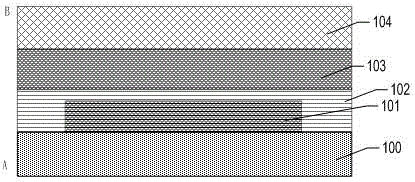
Examples
Example Embodiment
[0019] Example one
[0020] Surface roughness refers to the small spacing (Ry) and small peak and valley unevenness (Rz) of the surface, which is proportional to the surface tension. Surface roughening treatment is a physical or chemical method performed on the surface of a material in order to form surface roughness, such as a plasma treatment method.
[0021] Such as figure 1 As shown, a packaged device 101 is arranged on a substrate 100, and a first-level thin film layer 102, which is parylene, is deposited on top of the packaged device 101, and is plasma treated with argon in the dry etching chamber . A second-level thin-film layer 103, which is aluminum oxide, is deposited on the first-level thin-film layer 102, and is plasma treated with argon in the dry etching chamber. A third-level thin-film layer 104, which is parylene, is deposited on the second-level thin-film layer 103, and is plasma treated with argon in the dry etching chamber.
[0022] In the above-mentioned roughe...
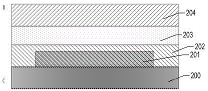
Example Embodiment
[0025] Example two
[0026] Chemical modification refers to the process of replacing a certain hydrophilic gene of the matrix material with a hydrophobic group by adsorption, coating, polymerization, chemical reaction and other methods to improve the hydrophobic properties of the material, such as fluorination or silicification. The concentration of surface chemical modification (such as fluorine concentration after fluorination or silicon concentration after silicification) is inversely proportional to surface tension.
[0027] Such as figure 2 As shown, a packaged device 201 is arranged on a substrate 200, and a first-level thin film layer 202, which is parylene, is deposited on top of the packaged device 201, and is fluorinated with CF4 gas in the dry etching chamber deal with. A second-level thin-film layer 203 is deposited on the first-level thin-film layer 202, which is aluminum oxide, and is fluorinated in the dry etching chamber using CF4 gas. A third-level thin-film lay...
Example Embodiment
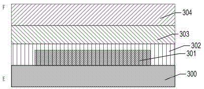
[0031] Example three
[0032] Such as image 3 As shown, a packaged device 301 is arranged on a substrate 300, and a first-level thin film layer 302 is deposited on the packaged device 301, which is graphene, and has a thermal conductivity of 5300 W / mK. A second-level thin-film layer 303 is deposited on the first-level thin-film layer 302, which is aluminum oxide and has a thermal conductivity of 45 W / mK. A third-level thin-film layer 304 is deposited on the second-level thin-film layer 303, which is silicon oxide and has a thermal conductivity of 7.6 W / mK.
[0033] By formula (among them Is the surface tension coefficient, Is the molar volume, Is a universal constant, Is the critical temperature when the surface tension is reduced to 0, and T is the temperature). It can be seen that temperature is inversely proportional to surface tension. Therefore, the film encapsulation structure will form a surface tension gradient that gradually increases from the E end to the F end, an...
PUM
| Property | Measurement | Unit |
|---|---|---|
| Diameter | aaaaa | aaaaa |
| Thermal conductivity | aaaaa | aaaaa |
| Thermal conductivity | aaaaa | aaaaa |
Abstract
Description
Claims
Application Information
 - R&D Engineer
- R&D Manager
- IP Professional
- Industry Leading Data Capabilities
- Powerful AI technology
- Patent DNA Extraction
Browse by: Latest US Patents, China's latest patents, Technical Efficacy Thesaurus, Application Domain, Technology Topic, Popular Technical Reports.
© 2024 PatSnap. All rights reserved.Legal|Privacy policy|Modern Slavery Act Transparency Statement|Sitemap|About US| Contact US: help@patsnap.com