
power conversion device

A power conversion device and semiconductor technology, applied in output power conversion devices, emergency protection circuit devices, conversion of AC power input to DC power output, etc., can solve problems such as discreteness, and achieve great practical advantages, simple structure and reliability. The effect of protective action

Active Publication Date: 2017-11-07
FUJI ELECTRIC CO LTD
View PDF2 Cites 0 Cited by
  • Summary
  • Abstract
  • Description
  • Claims
  • Application Information

AI Technical Summary

Problems solved by technology

However, the current supplied to the above-mentioned load M is actually a pulse current synchronized with the above-mentioned control signal, and the pulse current forms a discrete sine wave current waveform

Method used


Image

  • power conversion device
  • power conversion device
  • power conversion device

Examples


Embodiment Construction

[0033] Hereinafter, the above-mentioned power conversion device according to one embodiment of the present invention will be described with reference to the drawings.

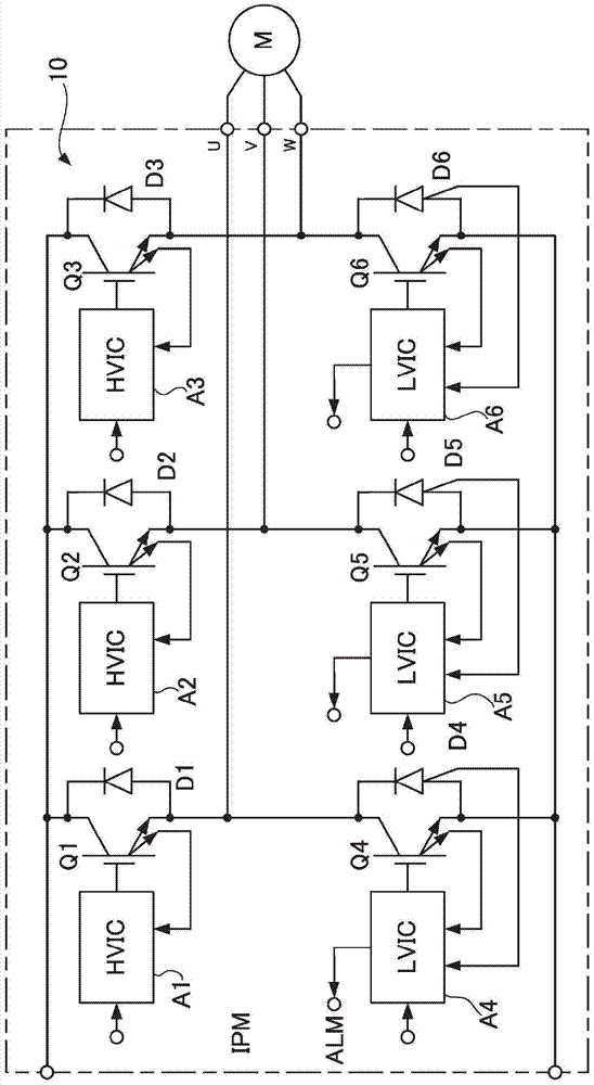
[0034] In this embodiment, the above-mentioned power conversion device such as figure 1 The main part of the main part of the power conversion device that constitutes the main body is shown in the schematic structure, which is basically the same as Figure 4 The structure of the shown existing power semiconductor module (IPM) 10 is the same. That is, the power semiconductor module (IPM) 10 constituting the main body of the power conversion device includes six semiconductor switching elements Q1, Q2 to Q6, and freewheeling diodes D1, D2 to D6 connected in antiparallel to the semiconductor switching elements Q1, Q2 to Q6. , and encapsulated. Each of the semiconductor switching elements Q1, Q2 to Q6 described above is composed of, for example, an IGBT.

[0035] The semiconductor switching elements Q1, Q2-Q6 and...


PUM


Abstract

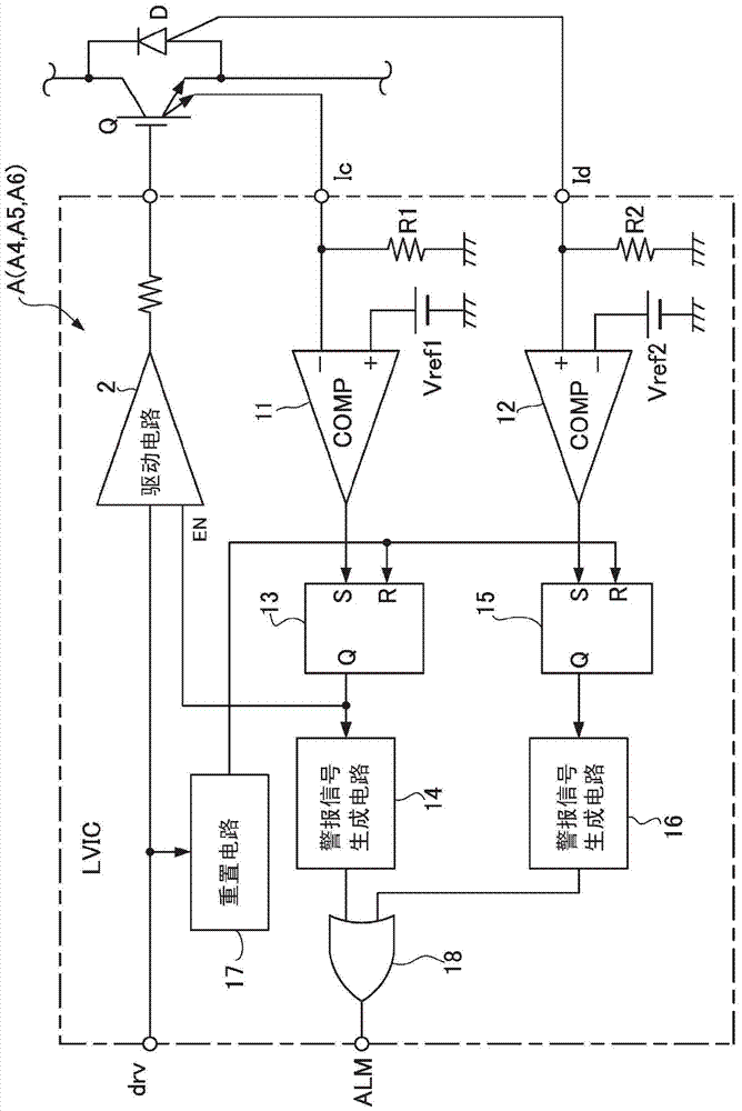
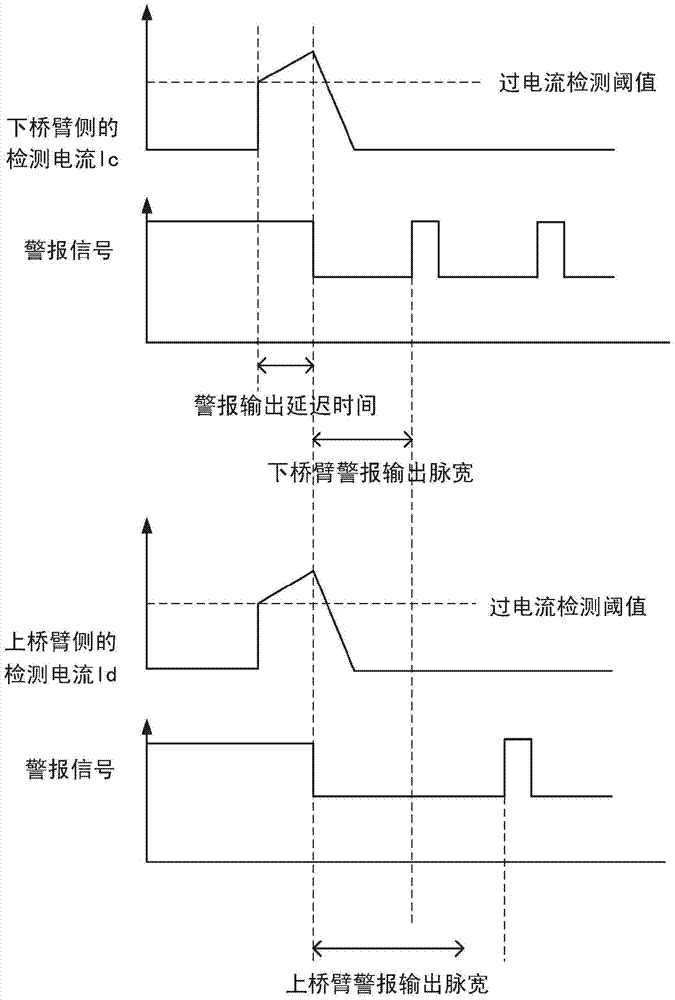
An overcurrent protection circuit that stops on / off driving of the semiconductor switching element when an overcurrent occurs in the semiconductor switching element is provided in the driving circuit for driving the semiconductor switching element of the lower arm of the half-bridge circuit. In addition, an alarm signal generating circuit is provided in the drive circuit of the lower arm, and the alarm signal generating circuit generates a first alarm signal when the overcurrent protection circuit of the lower arm operates, and flows to the lower arm when the overcurrent protection circuit operates. A second alarm signal is generated when the current of the freewheeling diode connected in anti-parallel of the semiconductor switching elements of the bridge arm exceeds the current limit value.

Description

technical field [0001] The present invention relates to a power conversion device provided with an overcurrent protection function for a semiconductor switching element constituting a main body of the power conversion device. Background technique [0002] A typical inverter device as a power conversion device has the following Figure 4 The main body of the power conversion device shown serves as a main body that drives a load M such as a three-phase AC motor. The main body of the power conversion device is as Figure 4 As shown in the schematic configuration diagram, the power semiconductor module (IPM) 10 is realized in the form of a power semiconductor module (IPM) 10 provided with, for example, six semiconductor switching elements Q1, Q2 to Q6 composed of IGBTs and packaged. This kind of inverter device is described in detail in Patent Document 1, for example, through a control circuit not shown, the above-mentioned semiconductor switching elements Q1, Q2-Q6 are connecte...

Claims


Application Information

Patent Timeline
Patent Type & Authority Patents(China)
IPC IPC(8): H02M1/32H02M7/5387
CPCH02M1/32H02M7/53871H02H7/1225H02M7/537
Inventor 高际和美
Owner FUJI ELECTRIC CO LTD
Learn More