Resistive non-volatile memory device and manufacturing method thereof

A non-volatile, manufacturing method technology, applied in the direction of electric solid devices, circuits, electrical components, etc., can solve the problems of slow operation speed, large operating voltage, poor data preservation, etc., and achieve the effect of good reliability.

Active Publication Date: 2018-01-26
WINBOND ELECTRONICS CORP
View PDF6 Cites 0 Cited by
  • Summary
  • Abstract
  • Description
  • Claims
  • Application Information

AI Technical Summary

Problems solved by technology

At present, the non-volatile memory on the market is still dominated by flash memory (Flash Memory), but it has disadvantages such as high operating voltage, slow operation speed, and poor data retention, which limit the future development of flash memory.

Method used


Image

  • Resistive non-volatile memory device and manufacturing method thereof
  • Resistive non-volatile memory device and manufacturing method thereof
  • Resistive non-volatile memory device and manufacturing method thereof

Examples


Embodiment Construction

[0029] Embodiments for practicing the invention are discussed in detail below. It will be appreciated that the embodiments provide many applicable inventive concepts, which can be implemented in wide variation. The specific embodiments discussed are merely intended to invent specific ways of using the embodiments and are not intended to limit the scope of the invention. In order to make the features of the present invention more comprehensible, the specific examples below are described in detail in conjunction with the accompanying drawings:

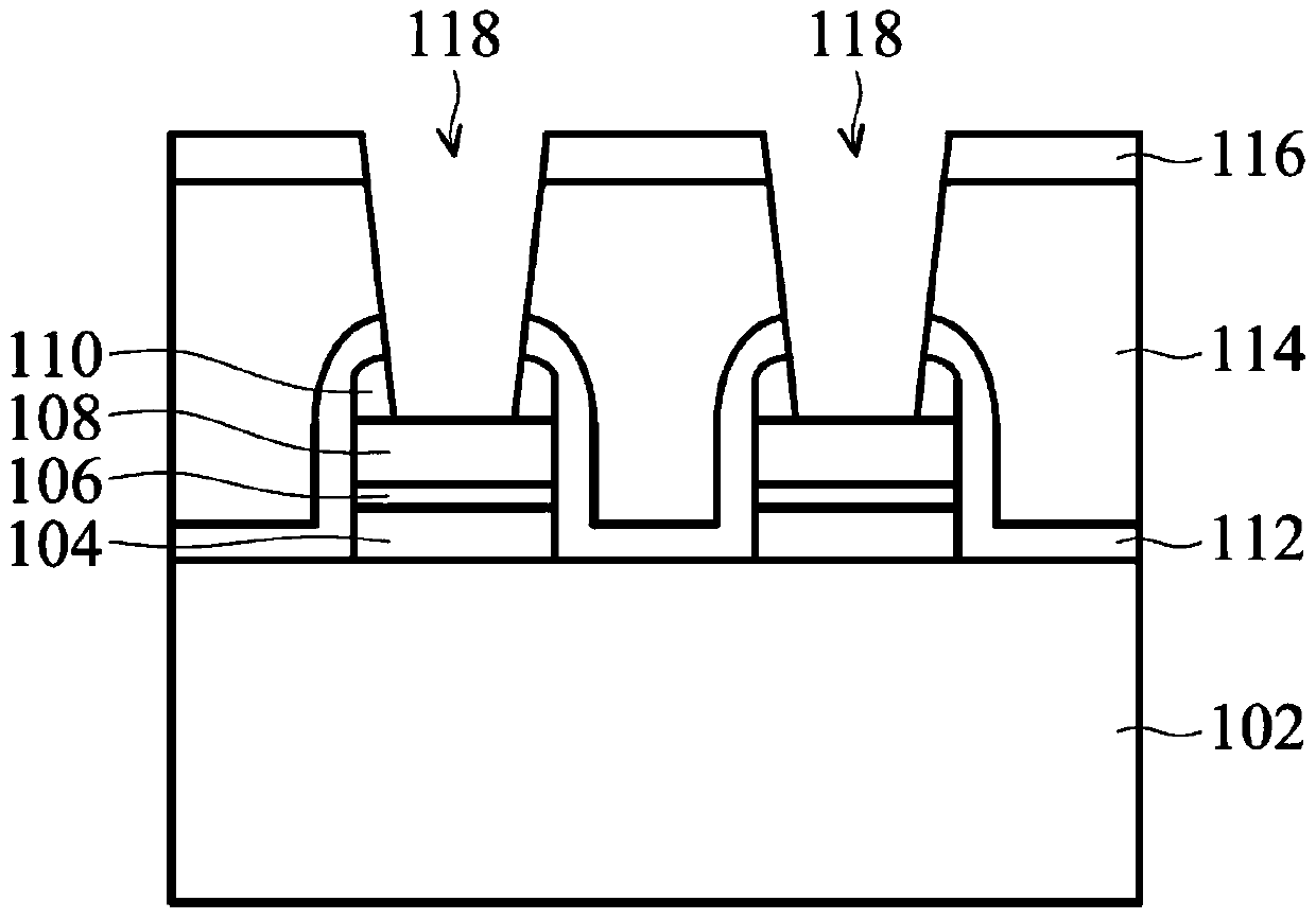
[0030] based on the following Figure 1A ~ Figure 1D A fabrication method of a resistive non-volatile memory device is disclosed. First, please refer to Figure 1A A substrate 102 is provided, and a lower electrode layer 104 , a resistance transition layer 106 and an upper electrode layer 108 are sequentially formed on the substrate 102 . Next, a first mask 110 is formed on the upper electrode layer 108 . Using the first mask 110 as ...


PUM

PropertyMeasurementUnit
thicknessaaaaaaaaaa
thicknessaaaaaaaaaa
thicknessaaaaaaaaaa

Abstract

A resistive non-volatile memory device and a manufacturing method thereof, the manufacturing method comprising: providing a substrate, wherein the substrate includes a lower electrode layer, a resistance switching layer, an upper electrode layer and a first mask; forming a layer The interlayer dielectric layer is above the substrate; forming a second mask on the interlayer dielectric layer; using the second mask as an etching mask, etching the interlayer dielectric layer to form an opening exposing the first mask ; forming a spacer layer on the bottom and sidewalls of the opening; removing part of the spacer layer on the bottom of the opening; performing an isotropic etching to remove part of the first mask in the opening. The invention can solve the problems related to the manufacturing process of the resistive non-volatile storage device and obtain better reliability.

Description

technical field [0001] The invention relates to a semiconductor device and a manufacturing method thereof, in particular to a resistive non-volatile memory device and a manufacturing method thereof. Background technique [0002] In recent years, consumer electronic products such as mobile phones, digital cameras and MP3 players have gradually become popular, which has greatly increased the demand for non-volatile memory. At present, the non-volatile memory in the market is still dominated by flash memory (Flash Memory), but it has disadvantages such as large operating voltage, slow operation speed, and poor data retention, which limit the future development of flash memory. [0003] Many new non-volatile memory materials and devices are being actively developed, including magnetic random access memory (MRAM), phase-change memory (OUM), and resistive memory (RRAM). Among them, resistive non-volatile memory has the advantages of low power consumption, low operating voltage, s...

Claims


Application Information

Patent Timeline
Patent Type & Authority Patents(China)
IPC IPC(8): H01L45/00H01L27/24
Inventor 吴伯伦沈鼎瀛李彦德
Owner WINBOND ELECTRONICS CORP
Why Eureka
Try Eureka