An array substrate, an embedded touch panel and a display device

A technology of array substrate and display area, which is applied in instruments, electrical digital data processing, input/output process of data processing, etc., can solve the problems of large signal noise and strong signal coupling effect, and achieves the improvement of signal-to-noise ratio and the reduction of signal Coupling effect, the effect of eliminating the phenomenon of screen jitter

Active Publication Date: 2017-07-07
BOE TECH GRP CO LTD +1
View PDF5 Cites 1 Cited by
  • Summary
  • Abstract
  • Description
  • Claims
  • Application Information

AI Technical Summary

Problems solved by technology

[0004] In view of this, the present invention provides an array substrate, an embedded touch panel and a display device to solve the problem of strong signal coupling between overlapping signal lines located in the non-display area of ​​the array substrate, resulting in The problem of high noise in the transmitted signal

Method used


Image

  • An array substrate, an embedded touch panel and a display device
  • An array substrate, an embedded touch panel and a display device
  • An array substrate, an embedded touch panel and a display device

Examples


Embodiment Construction

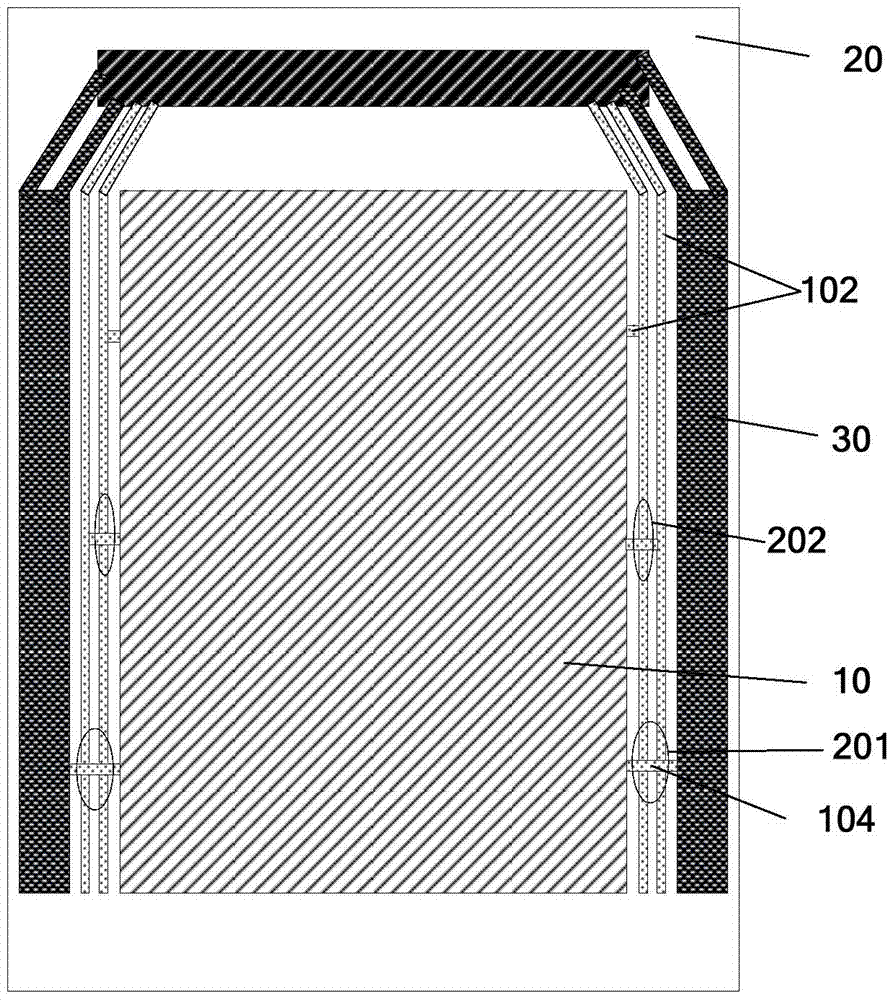
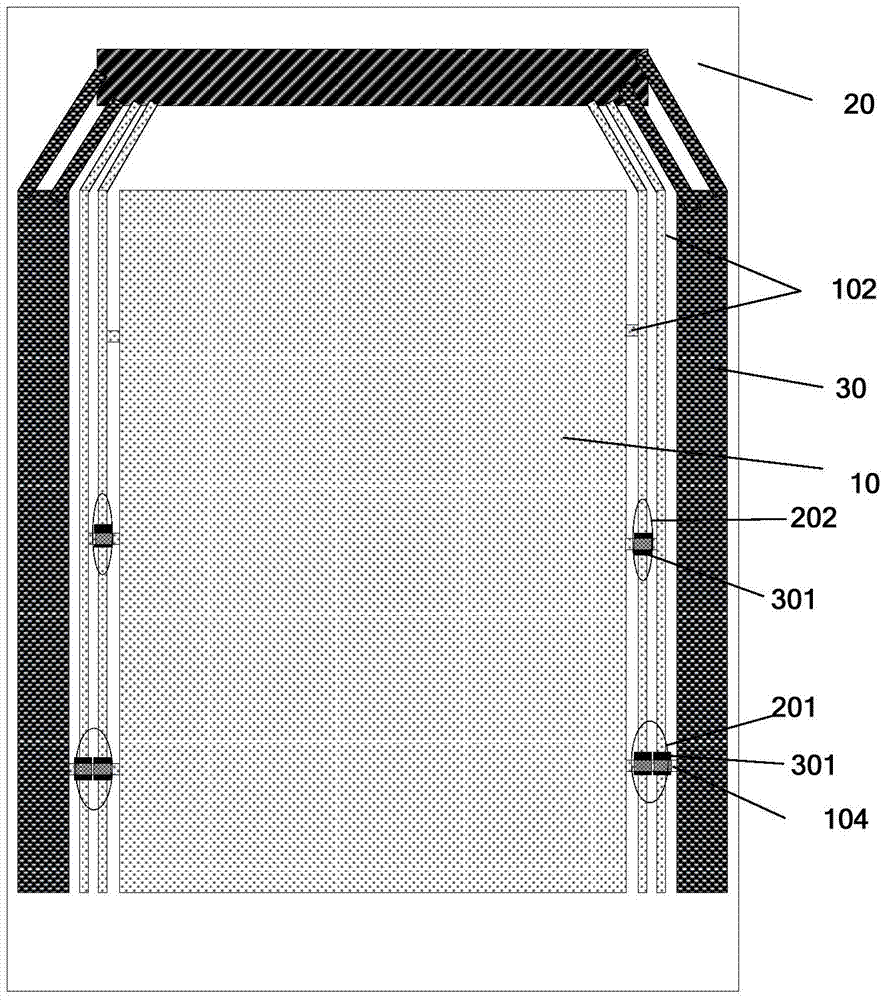
[0026] According to the capacitance calculation formula C=εs / d, it can be seen that the capacitance between two wires is determined by the overlapping area s between the two wires and the distance d between the two wires. When the overlapping area s is fixed, the capacitance between the two can be changed by changing the distance d between the two.

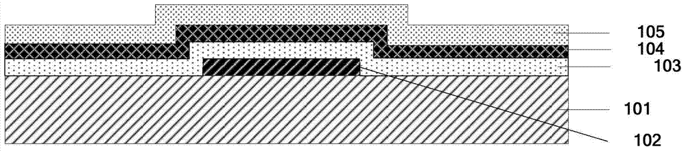
[0027] Therefore, in the embodiment of the present invention, in order to reduce the capacitance of the overlapping region of two signal traces located in the non-display area of ​​the array substrate, at least one elevated layer is added in the overlapping region of the two signal traces to change the capacitance in the overlapping region. The distance between the two signal traces in the area reduces the capacitance between them, reduces the signal coupling effect, improves the signal-to-noise ratio, and eliminates the image jitter phenomenon of the display device with the array substrate.

[0028] The specific implementation ma...


PUM


Abstract

The present disclosure provides an array substrate, an in-cell touch panel and a display device. The array substrate includes a display region and a non-display region. Gate lines, data lines, thin-film transistors and pixel electrodes are arranged at the display region, and each thin-film transistor includes a gate electrode, a gate insulation layer, an active layer, a source electrode and a drain electrode. First signal lines and second signal lines are arranged at the non-display region, and the first signal lines are located at a layer different from the second signal lines and intersect with the second signal lines. The first signal lines are arranged at a layer and made of a material identical to the gate lines. The gate insulation layer and at least one thickening layer are provided between the first signal lines and the second signal lines at overlapping regions of the first signal lines and the second signal lines.

Description

technical field [0001] The present invention relates to the field of display technology, in particular to an array substrate, an embedded touch panel and a display device. Background technique [0002] Please refer to figure 1 , figure 1 It is a structural schematic diagram of an array substrate of an in-cell touch panel in the prior art. The array substrate includes: a display area 10 and a non-display area 20 located on the periphery of the display area 10, and a GOA (Gate driver on array) is arranged in the non-display area. ) unit 30 and the touch driving electrode (TX) wiring 102, the GOA unit 30 is connected to the gate line (not shown) in the display area through the horizontal gate driving signal line 104, and the touch driving signal line 102 and Touch driving electrodes (not shown) located in the display area are connected. Due to the same non-display area, between the touch driving signal line 102 and the gate driving signal line 104, and between the horizontal...

Claims


Application Information

Patent Timeline
Patent Type & Authority Patents(China)
IPC IPC(8): G06F3/041
CPCG06F3/0412G06F3/04164G06F3/0418G06F3/0443G06F2203/04103G06F2203/04111
Inventor 曲连杰
Owner BOE TECH GRP CO LTD
Why Eureka
Try Eureka