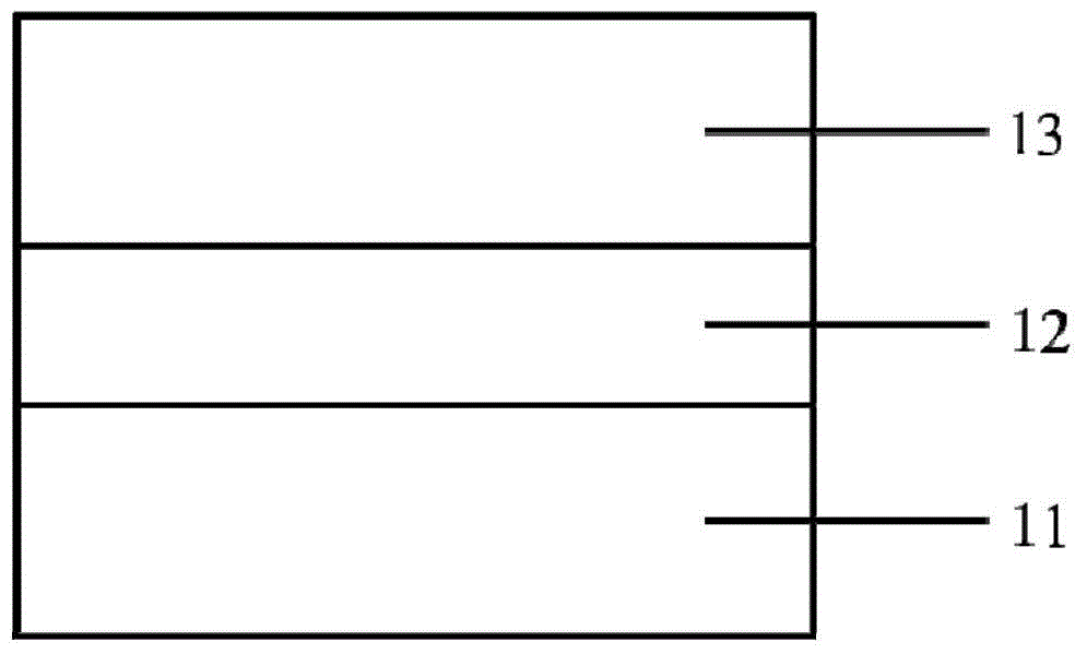
A kind of in growth on Si substrate 0.3 ga 0.7 as film and preparation method

A thin film and substrate technology, which is applied in the field of In0.3Ga0.7As thin film and its preparation, can solve the problems that it is difficult to precisely control the composition, thickness, and crystal quality, the structure of the buffer layer is complicated, and the growth steps are cumbersome, etc., and the buffer layer can be simplified. Effect of layer structure and epitaxial growth process, suppression of interface fluctuation, and simplification of epitaxial growth process

Active Publication Date: 2017-06-06
SOUTH CHINA UNIV OF TECH
View PDF3 Cites 0 Cited by
  • Summary
  • Abstract
  • Description
  • Claims
  • Application Information

AI Technical Summary

Problems solved by technology

The buffer layers of these multilayer structures have the characteristics of complex structure, thick thickness, and cumbersome growth steps, and it is difficult to precisely control the composition, thickness, and crystal quality of each layer of material, which affects the final In. 0.3 Ga 0.7 As film quality

Method used


Image

  • A kind of in growth on Si substrate  <sub>0.3</sub> ga  <sub>0.7</sub> as film and preparation method
  • A kind of in growth on Si substrate  <sub>0.3</sub> ga  <sub>0.7</sub> as film and preparation method
  • A kind of in growth on Si substrate  <sub>0.3</sub> ga  <sub>0.7</sub> as film and preparation method

Examples


Embodiment 1

[0036] The In grown on the Si substrate of this embodiment 0.3 Ga 0.7 The preparation method of As thin film comprises the following steps:

[0037] (1) Si substrate cleaning

[0038] The epitaxial substrate is an n-type Si substrate with (111) crystal orientation; after washing with acetone and deionized water, the organic matter on the substrate surface is removed; the Si substrate is placed in HF:H 2 O=1:10 solution sonicated for 3 minutes, concentrated H 2 SO 4 :H 2 o 2 :H 2 O=4:1:5 ultrasound for 10 minutes, HF:H 2 Ultrasound in O=1:10 solution for 3 minutes, and finally rinsed with deionized water to remove surface oxides and organic matter; the cleaned Si substrate was dried with high-purity nitrogen;

[0039] (2) Si substrate pretreatment

[0040] After the Si substrate is cleaned, it is sent to the molecular beam epitaxy sampling chamber for pre-degassing for 30 minutes; then sent to the transfer chamber for degassing at 400°C for 2 hours, and then sent to th...

Embodiment 2

[0052] The In grown on the Si substrate of this embodiment 0.3 Ga 0.7 The preparation method of As thin film comprises the following steps:

[0053] (1) Si substrate cleaning

[0054] The epitaxial substrate is an n-type Si substrate with (111) crystal orientation; after washing with acetone and deionized water, the organic matter on the substrate surface is removed; the Si substrate is placed in HF:H 2 O=1:10 solution sonicated for 1 minute, concentrated H 2 SO 4 :H 2 o 2 :H 2 O=4:1:5 Ultrasound for 5 minutes, HF:H 2 Ultrasound in O=1:10 solution for 1 minute, and finally rinsed with deionized water to remove surface oxides and organic matter; the cleaned Si substrate was dried with high-purity nitrogen;

[0055] (2) Si substrate pretreatment

[0056] After the Si substrate is cleaned, it is sent to the molecular beam epitaxy sampling chamber for pre-degassing for 15 minutes; then sent to the transfer chamber for degassing at 300°C for 0.5 hours, and then sent to the...


PUM

PropertyMeasurementUnit
thicknessaaaaaaaaaa
thicknessaaaaaaaaaa
surface roughnessaaaaaaaaaa

Abstract

The invention discloses an In0.3Ga0.7As thin film growing on a Si substrate. The In0.3Ga0.7As thin film comprises a low-temperature In0.28Ga0.72As buffering layer growing on the Si substrate and an In GaAs (Eg=1.0eV) epitaxial layer thin film body growing on the low-temperature buffering layer. The invention further discloses a preparing method for the InGaAs thin film growing on the Si substrate, and a molecular beam epitaxy growing method is adopted for the low-temperature growth of the In0.28Ga0.72As buffering layer, the annealing process of the buffering layer and the growth of the In0.3Ga0.7As epitaxial layer thin film body. The obtained In0.3Ga0.7As thin film is high in crystalline quality, flat in surface and of positive promote significance in preparation of semiconductor devices and particularly in the field of solar cells.

Description

technical field [0001] The invention relates to the field of preparation of InGaAs thin films, in particular to an InGaAs grown on a Si substrate 0.3 Ga 0.7 As thin film and its preparation method. Background technique [0002] III-V compounds are widely used in optoelectronic devices due to their advantages of good stability, small effective mass, high electron mobility and peak velocity, and high light absorption coefficient. Among them, In x Ga 1-x The band gap of As (0≤x≤1) material can vary in the range of 0.35eV (InAs)-1.43eV (GaAs) with the change of In composition. According to these characteristics, In x Ga 1-x As materials can be applied in the field of optoelectronic semiconductor devices such as high electron mobility transistors, photodiodes, and room temperature infrared detectors. Especially for specific components of In x Ga 1-x As material, because it is a direct bandgap semiconductor and has a specific bandgap width, it is widely used in some field...

Claims


Application Information

Patent Timeline
Patent Type & Authority Patents(China)
IPC IPC(8): H01L29/201H01L31/0304H01L21/02
CPCH01L21/02546H01L29/201H01L33/02
Inventor 李国强高芳亮温雷李景灵管云芳张曙光
Owner SOUTH CHINA UNIV OF TECH
Why Eureka
Try Eureka