Defect detection method and device of semiconductor device
- Summary
- Abstract
- Description
- Claims
- Application Information
AI Technical Summary
Problems solved by technology
Method used
Image
Examples
Embodiment Construction
[0023] As mentioned in the background, the existing defect detection methods are time-consuming, heavy workload and low accuracy.
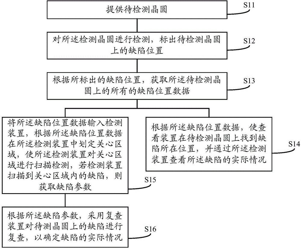
[0024] For details, please refer to figure 1 , is a flow diagram of a defect detection method, including:
[0025] Step S11, providing a wafer to be inspected;
[0026] Step S12, inspecting the inspected wafer, and marking defect positions on the inspected wafer;
[0027] Step S13, according to the marked defect position, obtain all defect position data on the wafer to be inspected;
[0028] After step S13, execute step S14 or S15, wherein:
[0029] Step S14, according to the defect location data, make the viewing device (such as a microscope) find the location of the defect on the wafer to be inspected, and use the inspection device to view the actual situation of the defect, such as the location of the semiconductor structure at the defect , the difference between structure, size and design standards;
[0030] Step S15, input the defect pos...
PUM
 Abstract
Description
Claims
Application Information
 - R&D
- Intellectual Property
- Life Sciences
- Materials
- Tech Scout
- Unparalleled Data Quality
- Higher Quality Content
- 60% Fewer Hallucinations
Browse by: Latest US Patents, China's latest patents, Technical Efficacy Thesaurus, Application Domain, Technology Topic, Popular Technical Reports.
© 2025 PatSnap. All rights reserved.Legal|Privacy policy|Modern Slavery Act Transparency Statement|Sitemap|About US| Contact US: help@patsnap.com


