Layered electrode matched with Mg-Si-Sn-based thermoelectric element and connecting technology thereof
A technology of mg-si-sn and thermoelectric elements, which is applied in the manufacture/processing of thermoelectric devices, materials for junction leads of thermoelectric devices, etc., can solve the problems of low performance of Si thermoelectric materials and difficulty in developing to the application stage, etc. Achieve the effect of simple and reliable process, good electrical property transition, and reduce interface thermal stress
- Summary
- Abstract
- Description
- Claims
- Application Information
AI Technical Summary
Problems solved by technology
Method used
Image
Examples
Embodiment 1
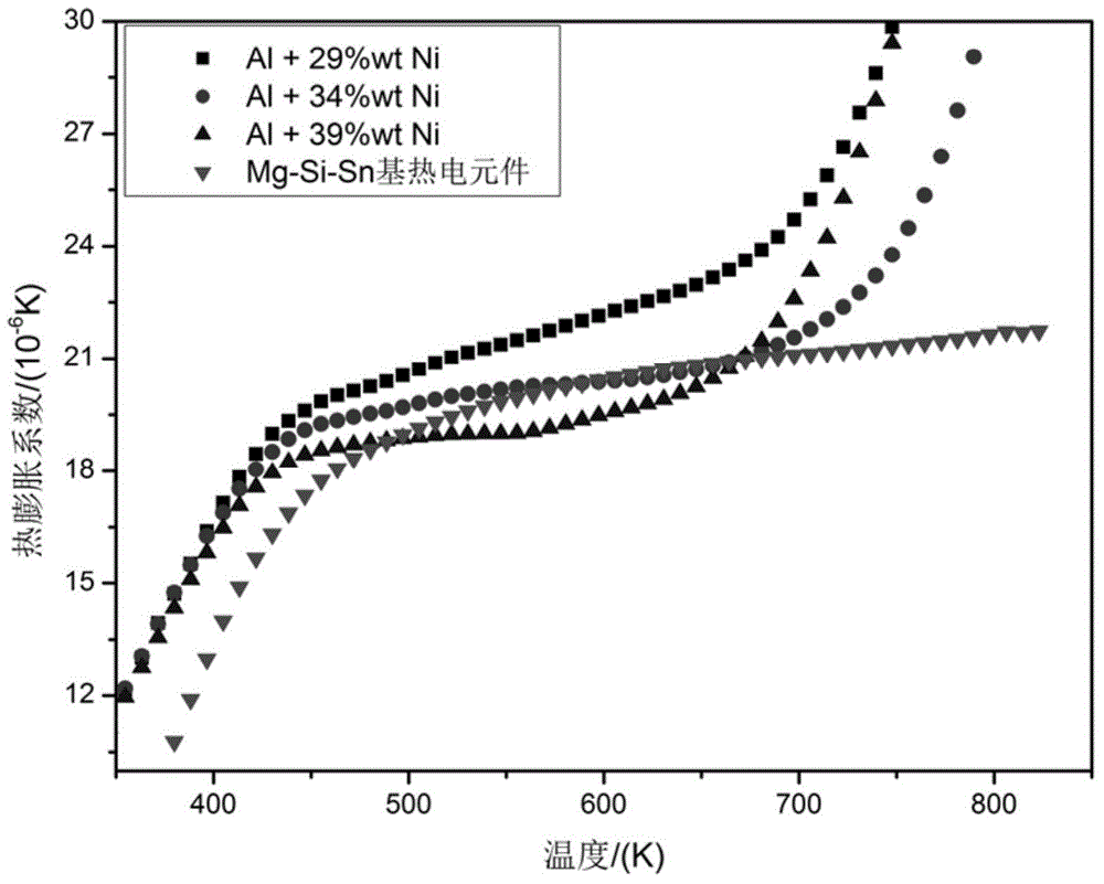
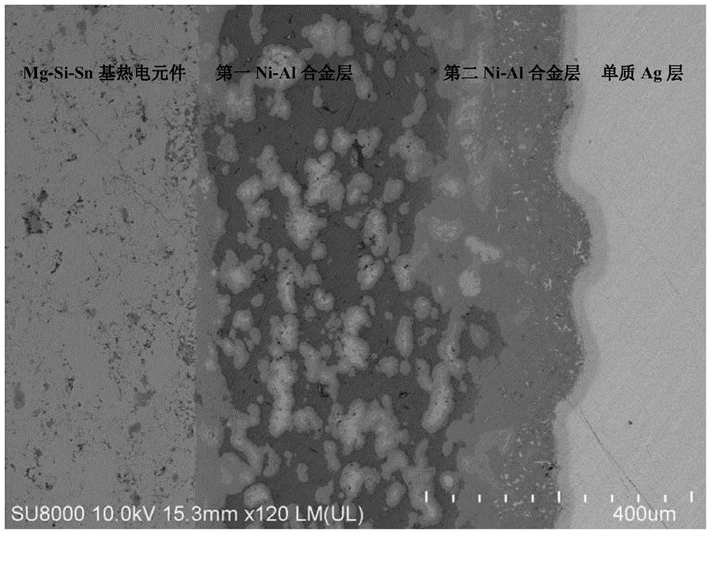
[0038] A multilayer electrode matched with a Mg-Si-Sn based thermoelectric element, the electrode is divided into a three-layer structure: first Ni-Al alloy layer, second Ni-Al alloy layer and elemental Ag layer. Wherein, the mass percent content of Ni element in the first Ni-Al alloy layer is 29%, the balance is Al element, and the thickness of the first Ni-Al alloy layer is 0.5mm; The Ni element in the second Ni-Al alloy layer The mass percentage is 42%, and the balance is Al element. The thickness of the second Ni-Al alloy layer is 0.15mm; the thickness of the simple Ag layer is 0.4mm.
[0039] The connection process of the multilayer electrode of the present invention and the Mg-Si-Sn base thermoelectric element is connected by spark plasma sintering (PAS), and the specific process steps are:
[0040] 1) Take 6.0g of Mg-Si-Sn-based thermoelectric material powder prepared by solid-state reaction, put it into a graphite mold for the first PAS sintering, the vacuum degree dur...
Embodiment 2
[0048] A multilayer electrode matched with a Mg-Si-Sn based thermoelectric element, the electrode is divided into a three-layer structure: first Ni-Al alloy layer, second Ni-Al alloy layer and elemental Ag layer. Wherein, the mass percent content of Ni element in the first Ni-Al alloy layer is 29%, the balance is Al element, and the thickness of the first Ni-Al alloy layer is 0.8mm; The Ni element in the second Ni-Al alloy layer The mass percentage is 59%, the balance is Al element, the thickness of the second Ni-Al alloy layer is 0.15mm; the thickness of the simple Ag layer is 0.6mm.
[0049] The connection process of the multilayer electrode of the present invention and the Mg-Si-Sn base thermoelectric element is connected by spark plasma sintering (PAS), and the specific process steps are:
[0050] 1) Take 6.0g of Mg-Si-Sn-based thermoelectric material powder prepared by solid-state reaction, put it into a graphite mold for the first PAS sintering, the vacuum degree during ...
Embodiment 3
[0058] A multilayer electrode matched with a Mg-Si-Sn based thermoelectric element, the electrode is divided into a three-layer structure: first Ni-Al alloy layer, second Ni-Al alloy layer and elemental Ag layer. Wherein, the mass percentage content of Ni element in the first Ni-Al alloy layer is 39%, the balance is Al element, and the thickness of the first Ni-Al alloy layer is 0.8mm; The Ni element in the second Ni-Al alloy layer The mass percentage content is 42%, the balance is Al element, the thickness of the second Ni-Al alloy layer is 0.15mm; the thickness of the simple Ag layer is 0.6mm.
[0059] The connection process of the multilayer electrode of the present invention and the Mg-Si-Sn base thermoelectric element is connected by spark plasma sintering (PAS), and the specific process steps are:
[0060] 1) Take 6.0g of Mg-Si-Sn-based thermoelectric material powder prepared by solid-state reaction, put it into a graphite mold for the first PAS sintering, the vacuum deg...
PUM
| Property | Measurement | Unit |
|---|---|---|
| thickness | aaaaa | aaaaa |
| thickness | aaaaa | aaaaa |
| thickness | aaaaa | aaaaa |
Abstract
Description
Claims
Application Information
 - Generate Ideas
- Intellectual Property
- Life Sciences
- Materials
- Tech Scout
- Unparalleled Data Quality
- Higher Quality Content
- 60% Fewer Hallucinations
Browse by: Latest US Patents, China's latest patents, Technical Efficacy Thesaurus, Application Domain, Technology Topic, Popular Technical Reports.
© 2025 PatSnap. All rights reserved.Legal|Privacy policy|Modern Slavery Act Transparency Statement|Sitemap|About US| Contact US: help@patsnap.com


