A method for optimizing a field-programmable gate array chip layout

A technology of chip layout and programming logic, applied in the direction of logic circuits using specific components, logic circuits using basic logic circuit components, etc., which can solve the problem of long processing time, large layout circuit volume, and failure to meet user requirements for program running time and other problems to achieve the effect of reducing the time and speeding up the running speed

Inactive Publication Date: 2015-02-11
CAPITAL MICROELECTRONICS
View PDF4 Cites 6 Cited by
  • Summary
  • Abstract
  • Description
  • Claims
  • Application Information

AI Technical Summary

Problems solved by technology

Therefore, when the simulated annealing layout algorithm deals with large-scale layout circuits, the processing time is too long due to the large size of the layout circuit, which often fails to meet the user's requirements for program running time.

Method used


Image

  • A method for optimizing a field-programmable gate array chip layout
  • A method for optimizing a field-programmable gate array chip layout
  • A method for optimizing a field-programmable gate array chip layout

Examples


Embodiment Construction

[0033] The technical solutions of the present invention will be described in further detail below with reference to the accompanying drawings and embodiments.

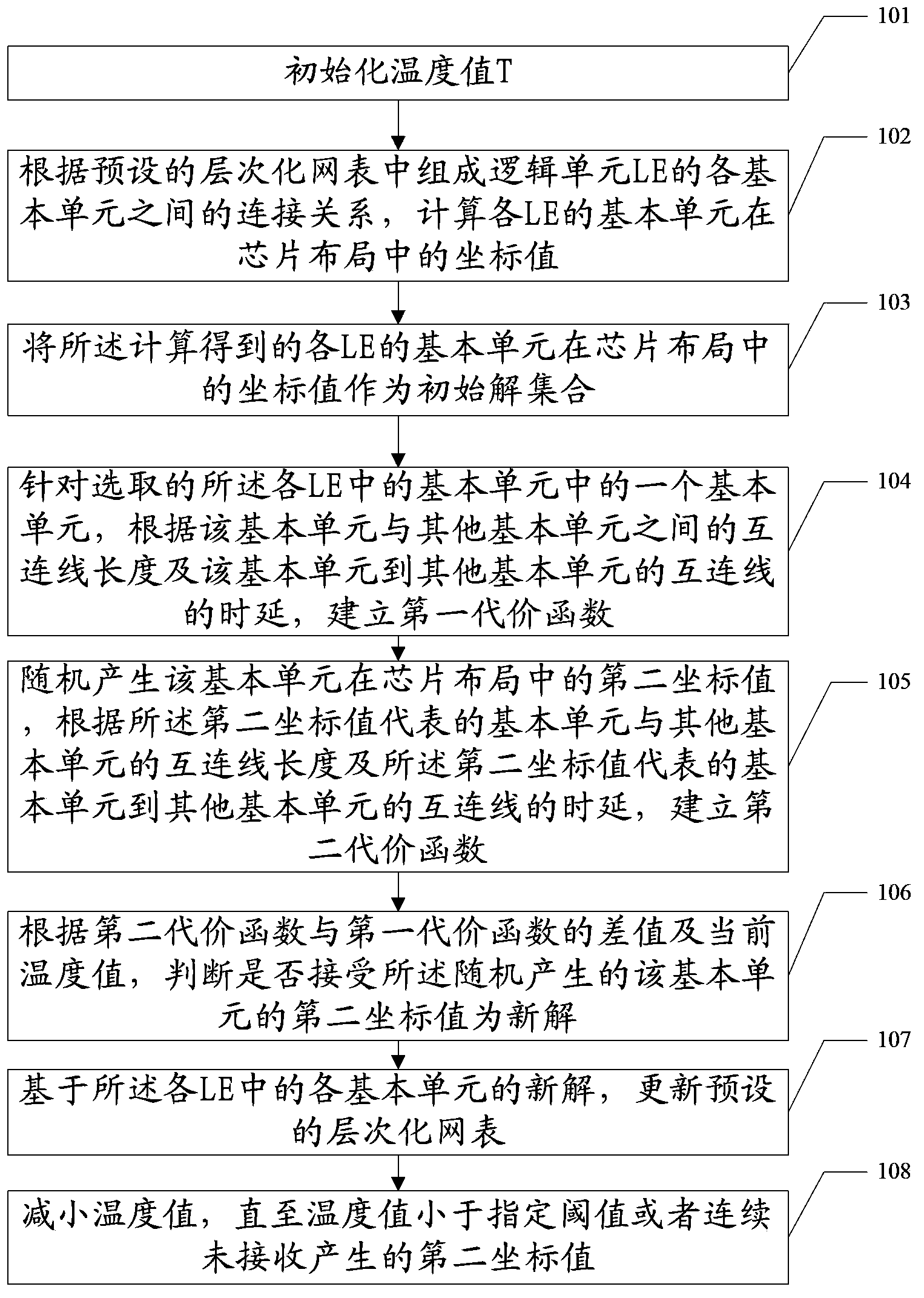
[0034] figure 1 It is a flow chart of the field programmable logic gate array chip layout optimization method of Embodiment 1 of the present invention. In the figure, the field programmable logic gate array chip layout optimization method mainly includes:

[0035] Step 101, initialize the temperature value T.

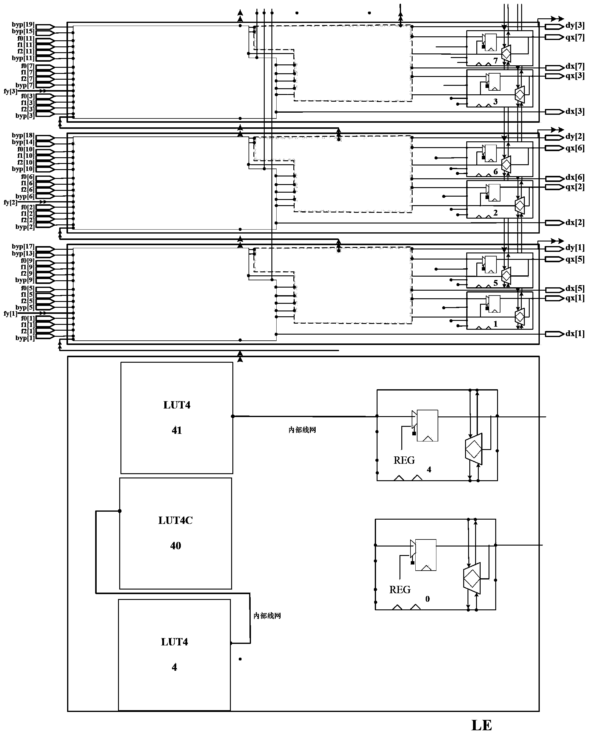
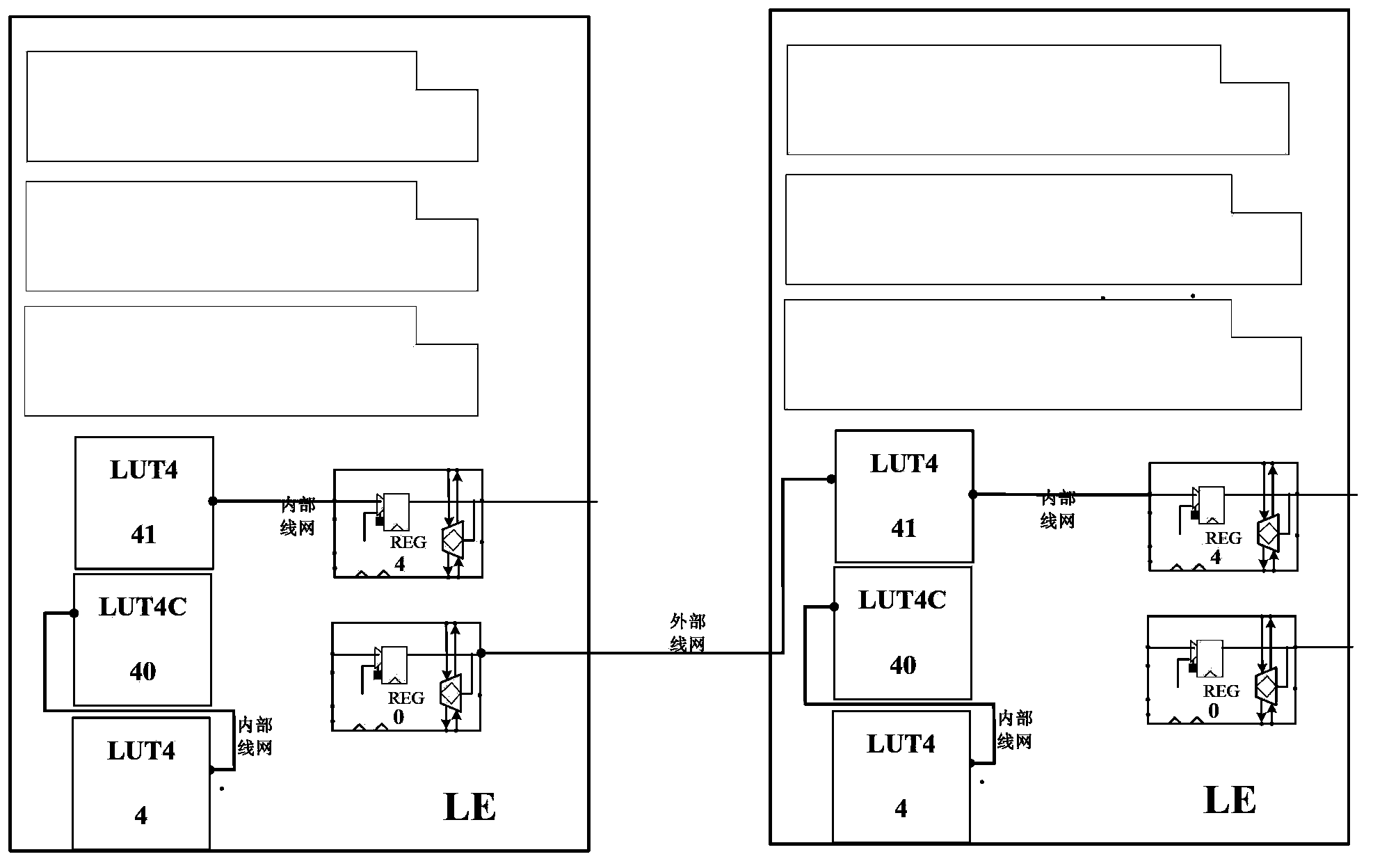
[0036] In step 101, the temperature T needs to be initialized, and the higher the value of the initialization temperature, the larger the search space. Specifically, the preset hierarchical netlist records the lookup table, the register, or the basic unit represented by the lookup table and the register and the logic unit composed of these basic units, and also records the connection relationship between these basic units. Initialize the temperature value T according to the formula Value, where the parameter...


PUM


Abstract

The invention relates to a method for optimizing a field-programmable gate array chip layout, the method comprising: initiating a temperature value T; selecting a basic unit, creating a first cost function in accordance with a length of an interconnection line between the basic unit and other basic units, and the time delay of the interconnection line; generating in random a second coordinate value of the basic unit, creating a second cost function in accordance with a length of an interconnection line between the basic unit represented by the second coordinate value and other basic units and the time delay of the interconnection line; determining whether the generated second coordinate value is accepted as a new solution according to a difference value of the second cost function from the first cost function and a current temperature value; based on the new solution of each basic unit in said each LE, updating a preset hierarchical net list; reducing the temperature value until the temperature value is less than a designated threshold value or the generated second coordinate value is continuously not received. When processing a layout circuit in a large scale, the method of optimizing a chip layout of the invention can speed up the running speed of the algorithm, and reduce the running time of a program.

Description

technical field [0001] The invention relates to a layout algorithm, in particular to a layout optimization method of a field programmable logic gate array chip. Background technique [0002] Currently, in Field Programmable Gate Array (Field Programmable Gate Array, FPGA) applications, integrated circuits are required to have a programmable or configurable interconnection network, and logic gates are connected to each other through the configurable interconnection network. FPGAs, functioning as stand-alone chips or as a core part of a system, have been widely used in a large number of microelectronic devices. The definition of FPGA logic gates in a broad sense not only refers to simple NAND gates, but also refers to logic units (LE, Logic Element) of combinational logic and sequential logic with configurable functions or logic composed of multiple logic units interconnected Piece. [0003] With the expansion of the scale of FPGA chips, the layout algorithm is becoming more...

Claims


Application Information

Patent Timeline
IPC IPC(8): H03K19/177
Inventor 蒋中华虞健刘桂林徐静刘明
Owner CAPITAL MICROELECTRONICS
Why Eureka
Try Eureka