Eureka AIR delivers breakthrough ideas for toughest innovation challenges, trusted by R&D personnel around the world.

Preparation method of chip type inductor

An inductor and chip technology, which is applied in the field of chip inductor preparation, can solve the problems of difficulty in identification of chip inductors, oxidation welding of welding heads, and high manufacturing costs, and achieves good constant temperature performance, high firmness, and reduced production. cost effect

Active Publication Date: 2015-02-04
GUANGDONG FENGHUA ADVANCED TECH HLDG
View PDF6 Cites 2 Cited by
  • Summary
  • Abstract
  • Description
  • Claims
  • Application Information

AI Technical Summary

Problems solved by technology

[0004] The terminal electrodes of traditional chip inductors are silver electrodes, and silver is a precious metal, so the cost is relatively high
At the same time, when the copper wire of the chip inductor is welded on the terminal electrode, the traditional alloy welding tip will oxidize when heated, which will cause poor welding, resulting in low pass rate and high manufacturing cost
Due to the miniaturization of chip inductors, it is currently only possible to print labels on the surface of inductors with a size of 1812 or larger, and the surface of inductors with a size of 0603-1812 series cannot be printed. The identification of type inductors is difficult

Method used


Image

  • Preparation method of chip type inductor
  • Preparation method of chip type inductor
  • Preparation method of chip type inductor

Examples


Embodiment Construction

[0029] In order to make the above objects, features and advantages of the present invention more obvious and comprehensible, specific implementations of the present invention will be described in detail below in conjunction with examples. In the following description, numerous specific details are set forth in order to provide a thorough understanding of the present invention. However, the present invention can be implemented in many other ways different from those described here, and those skilled in the art can make similar improvements without departing from the connotation of the present invention, so the present invention is not limited by the specific implementations disclosed below.

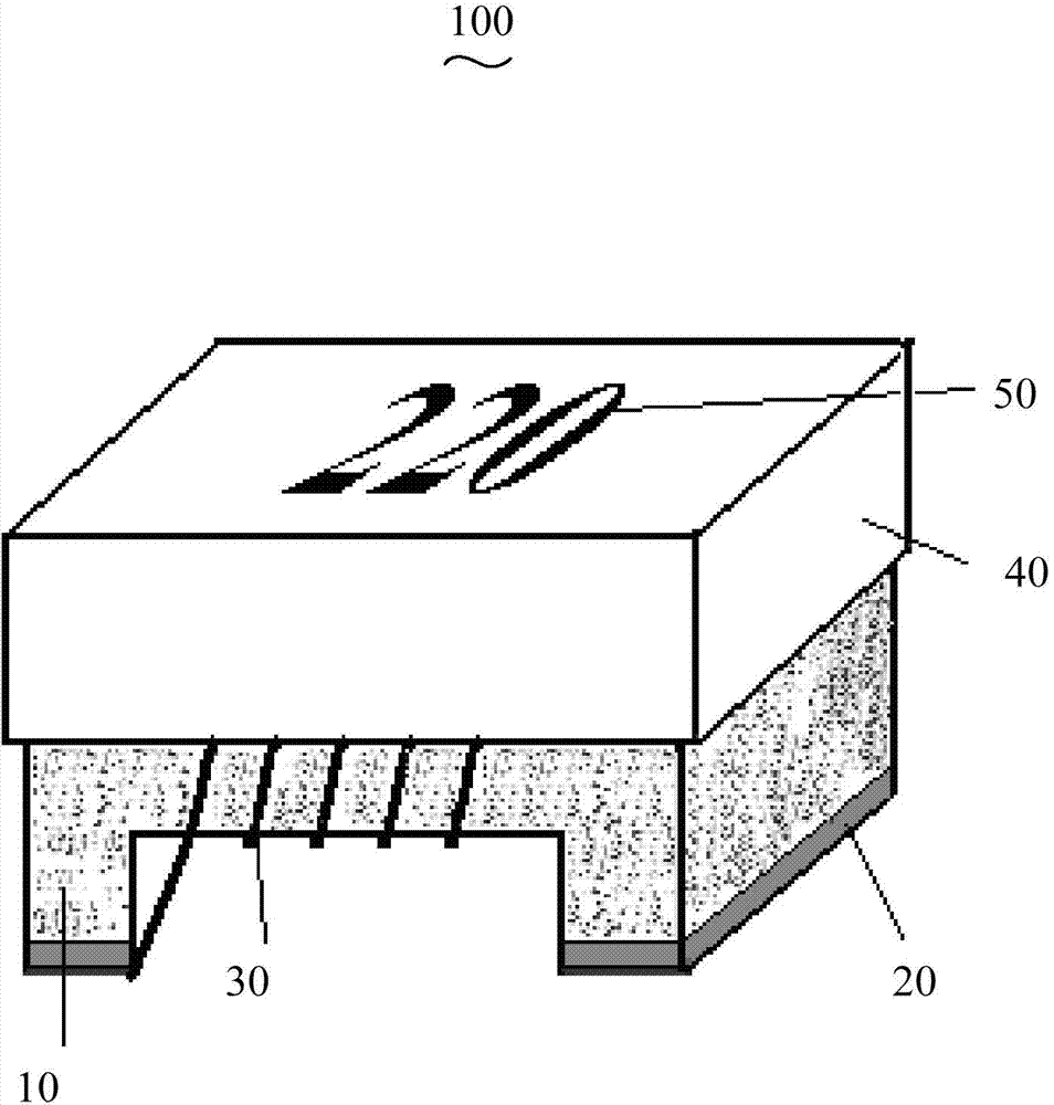
[0030] see figure 1 , The chip inductor 100 of one embodiment includes a magnetic core 10 , terminal electrodes 20 , an inductance coil 30 and a plastic encapsulation layer 40 .

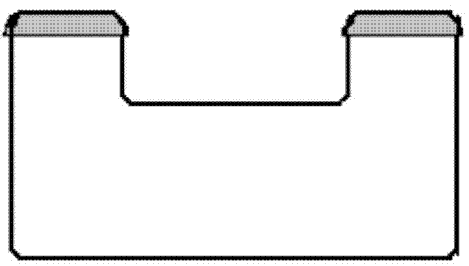
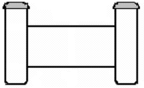
[0031] Chip inductors are U-shaped chip inductors or I-type chip inductors. The core structure of U-shaped ch...


PUM

PropertyMeasurementUnit
thicknessaaaaaaaaaa
thicknessaaaaaaaaaa

Abstract

The invention relates to a preparation method of a chip type inductor. The preparation method of the chip type inductor comprises the following steps: immersing one layer of copper slurry on two electrode end faces of a magnetic core of the chip type inductor; drying and sintering to form copper layers; sequentially electroplating the surfaces of the copper layers to form a nickel layer and a tin layer to form two end electrodes; winding a copper wire on a middle column part of the magnetic core of the chip type inductor to form an inductance coil and welding the two ends of the copper wire on the two end electrodes respectively in a manner of using a ceramic welding head to hotly press; forming a plastic sealing layer on one end, far away from the end electrodes, of the magnetic core; printing a mark on the surface of the plastic sealing layer in a manner of carrying out silk-screen printing by UV (Ultraviolet) printing ink; drying the chip type inductor printed with the mark. The preparation method of the chip type inductor has a lower cost and the prepared chip type inductor is convenient to recognize.

Description

technical field [0001] The invention relates to a preparation method of a chip inductor. Background technique [0002] An inductor is an energy storage element that converts electrical energy into magnetic field energy and stores energy in magnetic field energy. With the advancement of science and technology and the development of society, electronic equipment has become increasingly miniaturized, lightweight, and high-performance, which has promoted the development of surface mount technology, and chip electronic components have also developed rapidly. [0003] Chip inductors also become surface mount inductors. Like other chip components such as chip capacitors and chip resistors, they are a new generation of leadless or short lead microelectronic components suitable for surface mount technology. Its leading end and welding surface are on the same plane. [0004] The terminal electrodes of traditional chip inductors are silver electrodes, and silver is a precious metal, ...

Claims


Application Information

Patent Timeline
Patent Type & Authority Applications(China)
IPC IPC(8): H01F41/00H01F17/00H01F41/04H01F41/02B29C39/10
Inventor 区军沛周庆波李强徐建平
Owner GUANGDONG FENGHUA ADVANCED TECH HLDG
Why Eureka
Eureka Blog
Learn More