
Two-dimensional scanning micromirror of electrostatic drive microelectromechanical system

A micro-electro-mechanical system, electrostatic drive technology, applied in optical components, optics, instruments, etc., can solve the problems of large insertion loss, complex process, difficult wiring, etc., to eliminate mirror bending, simplify device structure and processing technology, and facilitate wiring. Effect

Active Publication Date: 2015-01-21
桂林光隆科技集团股份有限公司
View PDF6 Cites 10 Cited by
  • Summary
  • Abstract
  • Description
  • Claims
  • Application Information

AI Technical Summary

Problems solved by technology

[0003] The technical problem to be solved by the present invention is that the existing static-driven MEMS two-dimensional scanning micromirror has a large insertion loss, complex process, and difficult wiring when forming a large-scale micromirror array. It provides an electrostatically driven MEMS two-dimensional scanning Micromirror and its manufacturing process

Method used


Image

  • Two-dimensional scanning micromirror of electrostatic drive microelectromechanical system
  • Two-dimensional scanning micromirror of electrostatic drive microelectromechanical system
  • Two-dimensional scanning micromirror of electrostatic drive microelectromechanical system

Examples


Embodiment Construction

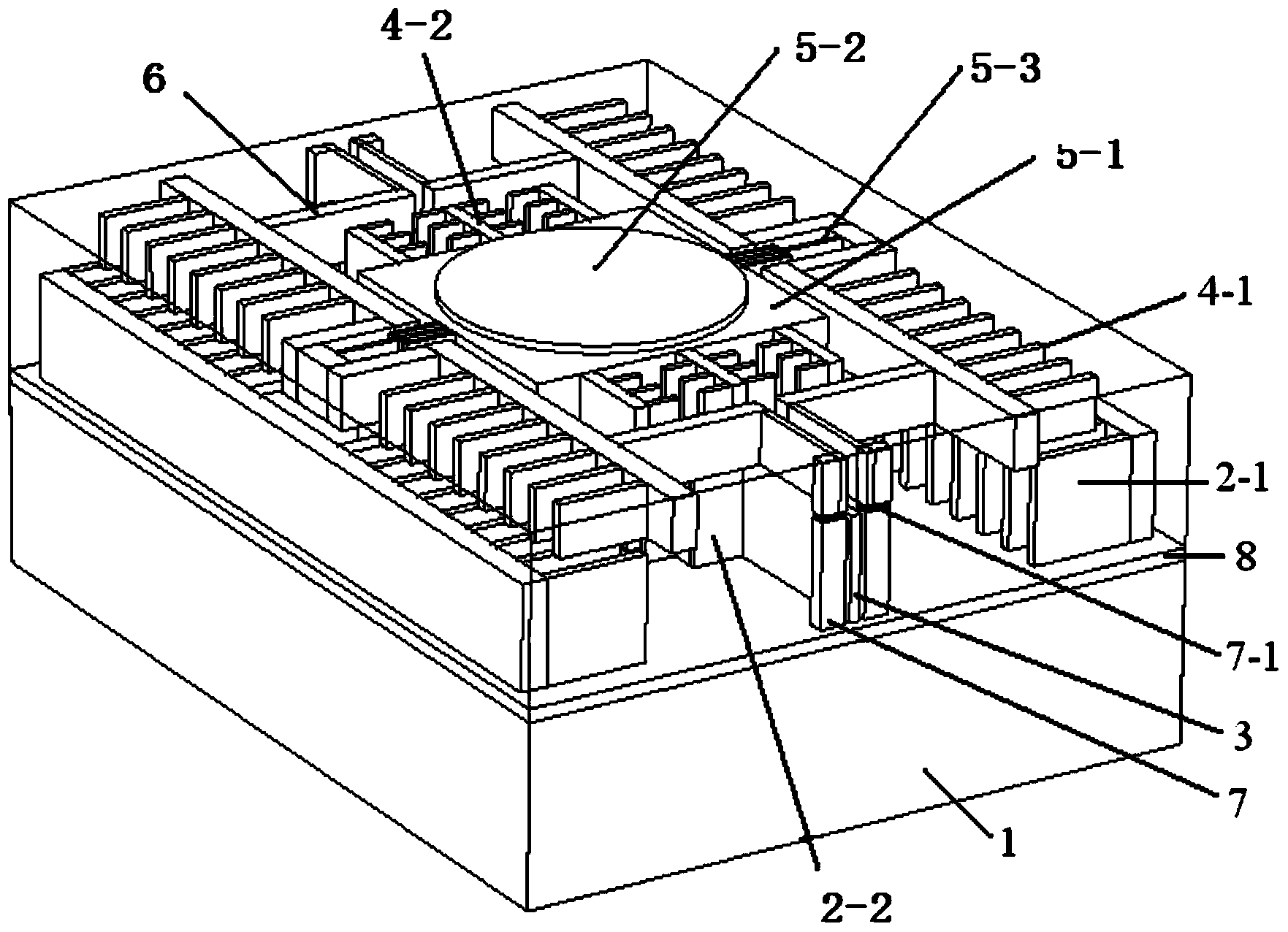
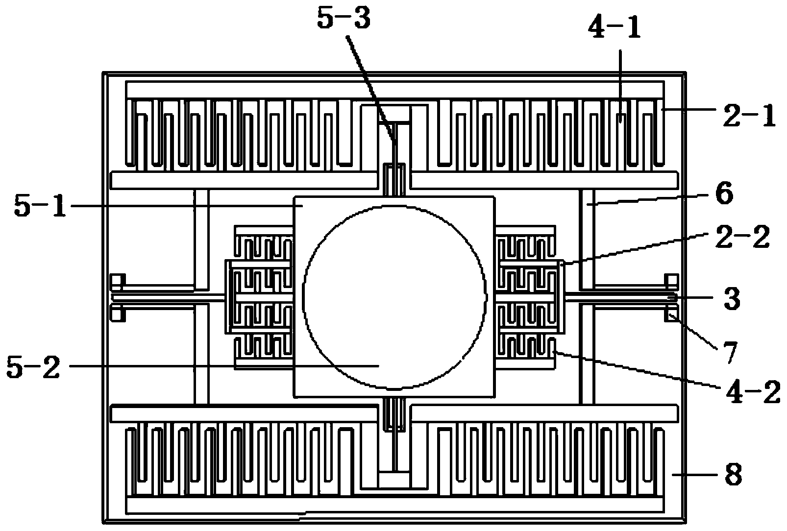
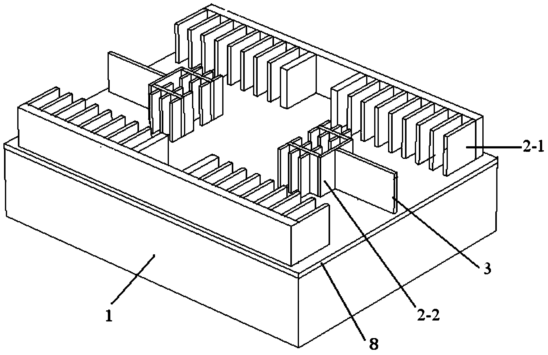
[0025] An electrostatically driven microelectromechanical system two-dimensional scanning micromirror, such as Figure 1-4 As shown, it is mainly composed of a low-resistance silicon substrate 1 at the bottom, fixed combs and comb leads 3 at the middle layer, movable combs at the top, two-dimensional scanning microlens 5-2 groups and support beam groups 6, and the anchor position 7 which is in the middle layer and the highest layer at the same time.

[0026] The upper surface of the low-resistance silicon substrate 1 is covered with an insulating layer 8 . The insulating layer 8 is polymer, silicon dioxide or silicon nitride with a thickness of 0.1-10 microns.

[0027] The fixed combs are fixed on the upper surface of the low-resistance silicon substrate 1, and consist of two outer fixed combs 2-1 and two inner fixed combs 2-2. Among them, two external fixed combs 2-1 are symmetrically arranged on the Y axis of the low-resistance silicon substrate 1, that is, at the edges of...


PUM


Abstract

The invention discloses a two-dimensional scanning micromirror of an electrostatic drive microelectromechanical system. The two-dimensional scanning micromirror mainly comprises a low-resistance silicon substrate located on the bottommost layer, fixed comb teeth, comb tooth leads, movable comb teeth, a two-dimensional scanning micromirror set, supporting beam sets and anchor positions, wherein the fixed comb teeth and the comb tooth leads are located on the middle layer, the movable comb teeth, the two-dimensional scanning micromirror set and the supporting beam sets are located on the topmost layer, and the anchor positions are located on both the middle layer and the topmost layer. Four L-shaped supporting beams are introduced in the X-axis direction as the mirror plane rotating shaft in the X-axis direction, so that the leads of the internal fixed comb teeth just pass through the center of the gap between every two adjacent L-shaped supporting beams. Due to the design, the device structure and the machining technology can be simplified, cost is reduced, the leads of the micromirror can be led more conveniently, and thus a large-scale micromirror array can be formed conveniently. The two-dimensional scanning micromirror is of vital significance in expanding the application fields of two-dimensional scanning micromirrors of electrostatic drive microelectromechanical systems.

Description

technical field [0001] The invention relates to the field of micro-opto-electro-mechanical systems, in particular to an electrostatically driven micro-electro-mechanical system two-dimensional scanning micromirror. Background technique [0002] In the field of micro-opto-electro-mechanical systems, electrostatically driven two-dimensional scanning micro-electro-mechanical system micro-lenses are important devices in modern optical communication systems, and can be used as optical switches, optical attenuators, and optical multiplexers. However, the existing electrostatically driven MEMS two-dimensional scanning micromirrors and their arrays mainly have the following disadvantages: (1) mirror bending caused by residual stress will be aggravated by temperature changes, resulting in increased insertion loss; (2) The device structure and processing technology are complicated, and the processing cost is high; (3) the leads are inconvenient when forming an array. These shortcomin...

Claims


Application Information

Patent Timeline
Patent Type & Authority Applications(China)
IPC IPC(8): G02B26/10
Inventor 陈春明胡放荣张隆辉彭晖
Owner 桂林光隆科技集团股份有限公司
Learn More