Transmission-type X-ray photoelectric cathode
A photocathode, X-ray technology, applied in the directions of X-ray tube electrodes, X-ray tubes, X-ray tube parts, etc., can solve the problems of inability to distribute information back out, unable to establish and so on
- Summary
- Abstract
- Description
- Claims
- Application Information
AI Technical Summary
Problems solved by technology
Method used
Image
Examples
Embodiment 1
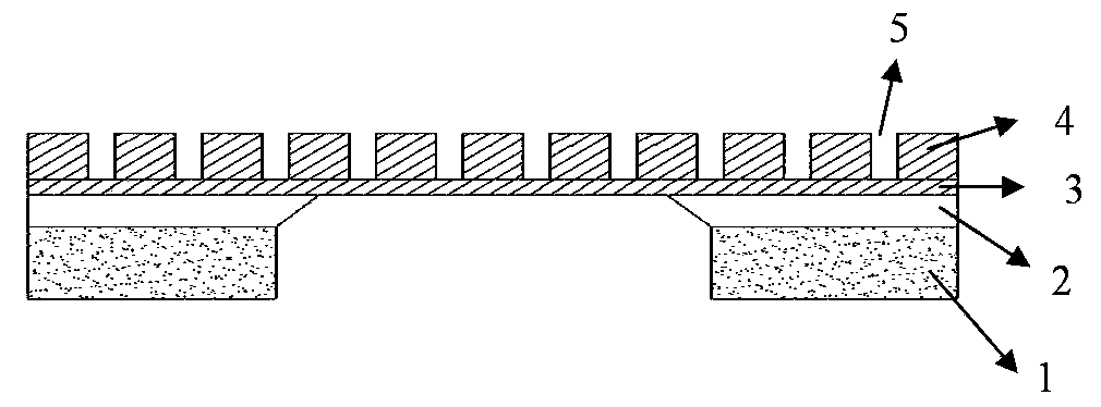
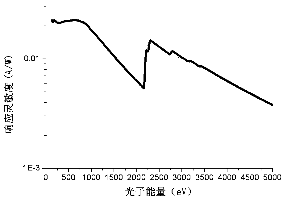
[0026] The gold layer I3 of the transmission X-ray photocathode has a thickness of 40nm, the gold layer II4 has a thickness of 360nm, and the area ratio of the microholes 5 is 1\8. image 3 is the energy response curve of the photocathode in the energy range of 100eV-5000eV. The method of making the cathode is as follows:
[0027] Step 1: prepare a clean silicon wafer as the cathode substrate, and use the method of spin coating on the substrate (the specific method and material selection can be found in relevant public documents, which will not be described in detail here), and deposit a polyimide film with a thickness of several microns as connection layer;
[0028] Step 2: Deposit a gold layer I with a thickness of 40nm on the polyimide film layer by means of electron beam evaporation or magnetron sputtering (for specific methods and material selection, please refer to relevant public documents, which will not be described in detail here);
[0029] Step 3: Spin-coat and de...
Embodiment 2
[0033] The gold layer I3 of the transmission type X-ray photocathode has a thickness of 40nm, the thickness of the gold layer II4 is 360nm, and the area ratio of the micropores 5 is 1\6. Figure 6 is the energy response curve of the photocathode in the energy range of 100eV-5000eV. The method of making negative electrode is the same as embodiment 1.
Embodiment 3
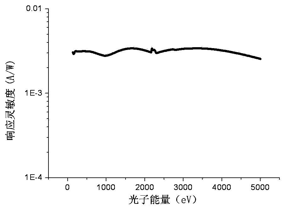
[0035] The gold layer I3 of the transmission X-ray photocathode has a thickness of 40nm, the gold layer II4 has a thickness of 400nm, and the area ratio of the microholes 5 is 1\8. Figure 4 is the energy response curve of the photocathode in the energy range of 100eV-5000eV. The method of making negative electrode is the same as embodiment 1.
PUM
| Property | Measurement | Unit |
|---|---|---|
| Thickness | aaaaa | aaaaa |
| Thickness | aaaaa | aaaaa |
| Thickness | aaaaa | aaaaa |
Abstract
Description
Claims
Application Information
 - R&D Engineer
- R&D Manager
- IP Professional
- Industry Leading Data Capabilities
- Powerful AI technology
- Patent DNA Extraction
Browse by: Latest US Patents, China's latest patents, Technical Efficacy Thesaurus, Application Domain, Technology Topic, Popular Technical Reports.
© 2024 PatSnap. All rights reserved.Legal|Privacy policy|Modern Slavery Act Transparency Statement|Sitemap|About US| Contact US: help@patsnap.com


