
A level conversion circuit

A technology for converting circuits and levels, which is applied in the direction of logic circuit connection/interface layout, logic circuit coupling/interface using field effect transistors, etc. It can solve the problem that the level conversion circuit cannot output negative voltage, etc., and achieve low cost, The effect of simple process

Active Publication Date: 2017-09-05
上海芯导电子科技股份有限公司
View PDF5 Cites 0 Cited by
  • Summary
  • Abstract
  • Description
  • Claims
  • Application Information

AI Technical Summary

Problems solved by technology

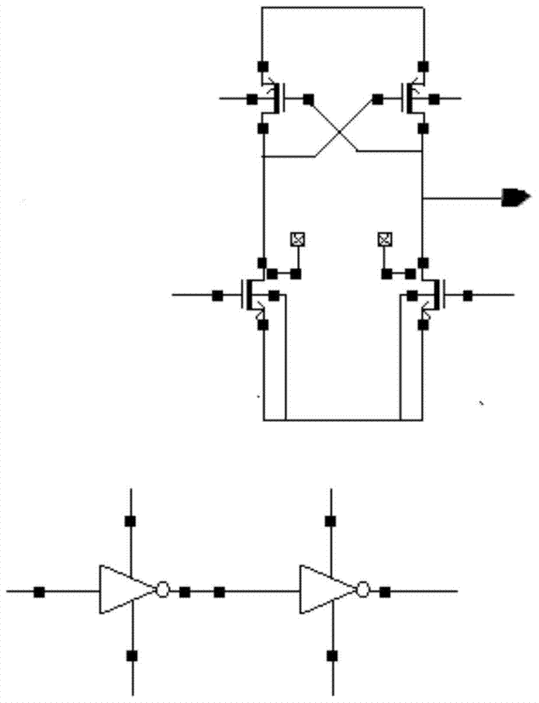
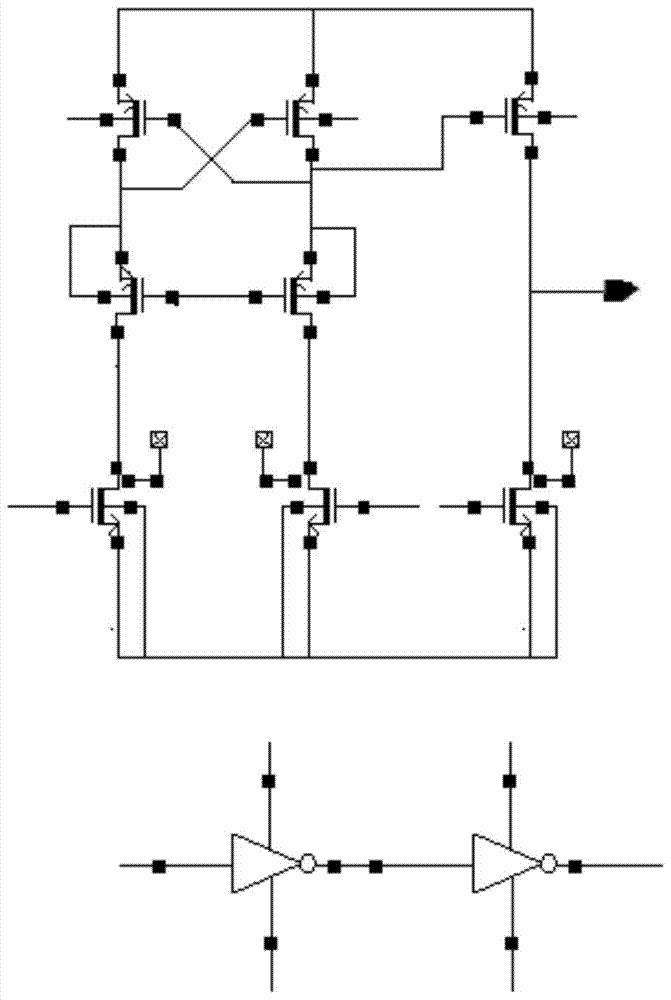
[0007] In order to solve the problem that the level conversion circuit in the prior art cannot output negative voltage under the non-epi process condition, the present invention provides a level conversion circuit, which is used to make the output voltage between positive voltage and negative voltage according to the transformation of the input signal Switch output between

Method used


Image

  • A level conversion circuit
  • A level conversion circuit
  • A level conversion circuit

Examples


Embodiment Construction

[0024] In order to explain the embodiments of the present invention or the technical solutions in the prior art more clearly, the following briefly introduces the accompanying drawings that need to be used in the description of the embodiments or the prior art. Obviously, the accompanying drawings in the following description are only These are some embodiments of the present invention. For those of ordinary skill in the art, other drawings can also be obtained according to these drawings without creative efforts.

[0025] It should be noted that, in the embodiments of the present invention, the P-channel metal oxide semiconductor field effect transistors are collectively referred to as P transistors, and the N-channel metal oxide semiconductor field effect transistors are collectively referred to as N transistors.

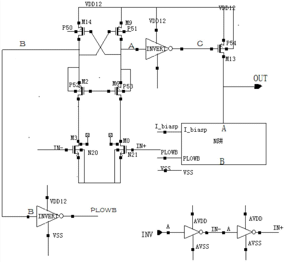
[0026] As a specific example, as image 3 As shown, it is a level conversion circuit according to an embodiment of the present invention. image 3 Among them, IN...


PUM


Abstract

The invention discloses a level conversion circuit. The level conversion circuit solves the problem that the level conversion circuit of the prior art is incapable of outputting a negative voltage under non-epi technique conditions. The level conversion circuit is used for switching output voltage between positive voltage and negative voltage according to input signal conversion. According to the level conversion circuit, the level conversion which covers a positive voltage domain and a negative voltage domain is realized through an N trap conversion structure. The level conversion circuit is capable of realizing the level conversion for any input voltage, the technique is simple, and the realizing cost is low.

Description

technical field [0001] The present invention relates to the technical field of integrated circuits, in particular to a level conversion circuit. Background technique [0002] During the operation of the integrated circuit, in order to adapt to various application scenarios, different voltages are often required. For example, in the LCD drive, it is necessary to work in a positive and negative voltage level conversion circuit, but the input voltage of the circuit is often single. Therefore, When designing integrated circuits, it is often necessary to convert input voltages into corresponding voltages for different application scenarios. [0003] In the prior art, the integrated circuits of LCD and other chips usually adopt the CMOS process, and with the improvement of the technological level, the circuit integration degree is continuously improved, the size and operating voltage of a single device are decreasing, and the breakdown voltage of MOS devices is gradually decreasin...

Claims


Application Information

Patent Timeline
Patent Type & Authority Patents(China)
IPC IPC(8): H03K19/0185
Inventor 肖晗符志岗朱同祥欧新华孙志斌陈敏袁琼
Owner 上海芯导电子科技股份有限公司
Learn More