Programmable fully-differential gain-bootstrap operational transconductance amplifier
A transconductance amplifier, fully differential technology, used in differential amplifiers, DC-coupled DC amplifiers, etc., can solve the problem of low power consumption efficiency, single-stage sleeve/folding amplifier open-loop gain is not large enough, single-stage gain bootstrap Amplifier bandwidth is small and other problems, to achieve the effect of increasing the input range
- Summary
- Abstract
- Description
- Claims
- Application Information
AI Technical Summary
Problems solved by technology
Method used
Image
Examples
Embodiment approach
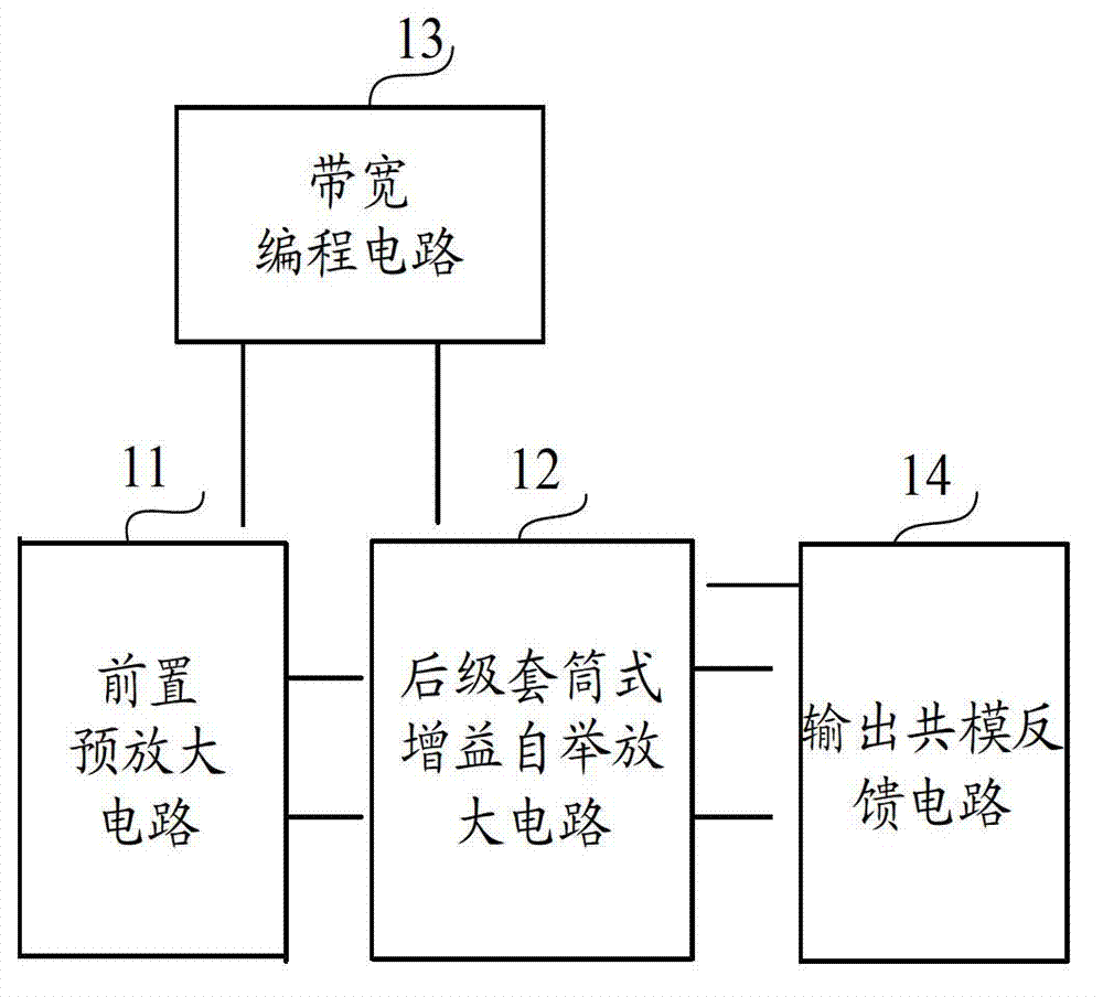
[0069] According to a specific implementation manner, the non-inverting output terminal of the pre-amplifier circuit is connected to the non-inverting input end of the rear-stage telescopic gain bootstrap amplifier circuit; the inverting output terminal of the pre-amplifier circuit The end is connected with the inverting input end of the rear-stage telescopic gain bootstrap amplifier circuit;
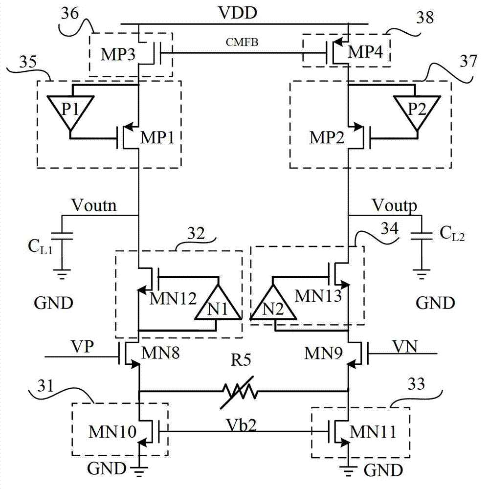
[0070] The non-phase output terminal of the post-stage telescopic gain bootstrap amplifier circuit and the positive-phase signal load to be driven by the programmable full differential gain bootstrap transconductance amplifier and the non-phase output detection of the output common-mode feedback circuit terminal connection; the inverting output terminal of the post-stage sleeve type gain bootstrap amplifier circuit is connected with the inverting signal load to be driven by the programmable fully differential gain bootstrap transconductance amplifier and the output common-mode feedback c...
specific Embodiment approach
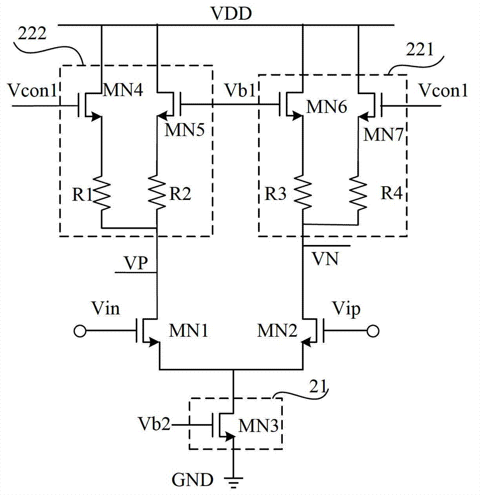
[0074] Such as figure 2 As shown, according to a specific implementation manner, the pre-amplification circuit includes:
[0075] a first bias current source 21, configured to provide a bias current;
[0076] The positive input transistor MN1, the gate is connected to the positive input voltage Vip, the source is connected to the ground terminal GND of the bias current source 21, the drain is connected to the high-level output terminal VDD of the driving power supply through the positive variable load network 221, and the source Extremely the inverting output terminal VN of the pre-amplification circuit;
[0077] Negative input transistor MN2, the gate is connected to the negative input voltage Vin, the source is connected to the ground terminal GND of the bias current source 21, the drain is connected to the high-level output terminal VDD of the driving power supply through the negative variable load network 222, and the source It is the positive phase output terminal VP o...
PUM
 Abstract
Description
Claims
Application Information
 - R&D Engineer
- R&D Manager
- IP Professional
- Industry Leading Data Capabilities
- Powerful AI technology
- Patent DNA Extraction
Browse by: Latest US Patents, China's latest patents, Technical Efficacy Thesaurus, Application Domain, Technology Topic, Popular Technical Reports.
© 2024 PatSnap. All rights reserved.Legal|Privacy policy|Modern Slavery Act Transparency Statement|Sitemap|About US| Contact US: help@patsnap.com


