visible light sensor

A visible light and sensor technology, which is applied in the direction of electric solid-state devices, semiconductor devices, semiconductor/solid-state device components, etc., can solve the problems of weak anti-infrared interference ability, achieve good linearity, simple peripheral circuits, and save costs.

Active Publication Date: 2017-05-10
吴晓龙
View PDF8 Cites 0 Cited by
  • Summary
  • Abstract
  • Description
  • Claims
  • Application Information

AI Technical Summary

Problems solved by technology

[0004] In order to overcome the deficiencies of the prior art, the present invention provides an anti-infrared photosensitive receiving device packaging material and a visible light sensor, and its purpose is to solve the problem that the existing photosensitive receiving device has weak anti-infrared interference ability

Method used


Image

  • visible light sensor
  • visible light sensor
  • visible light sensor

Examples


Embodiment Construction

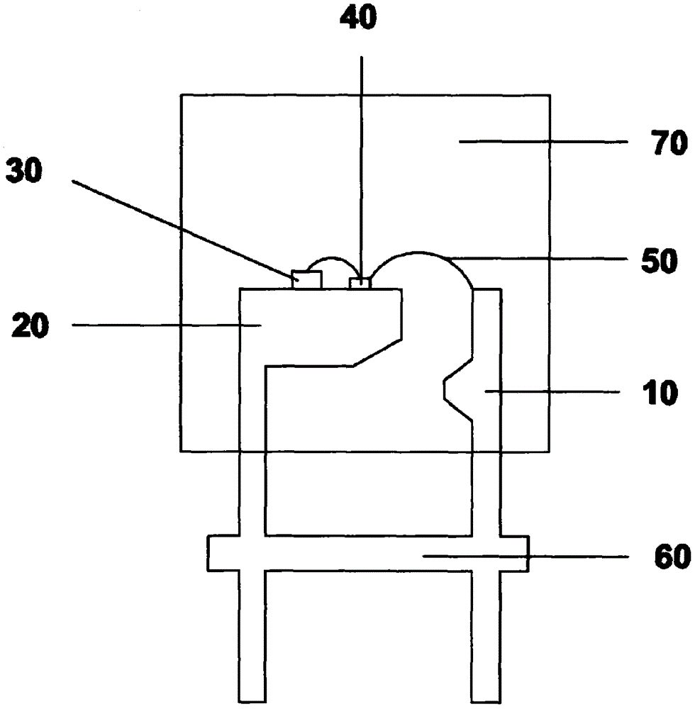
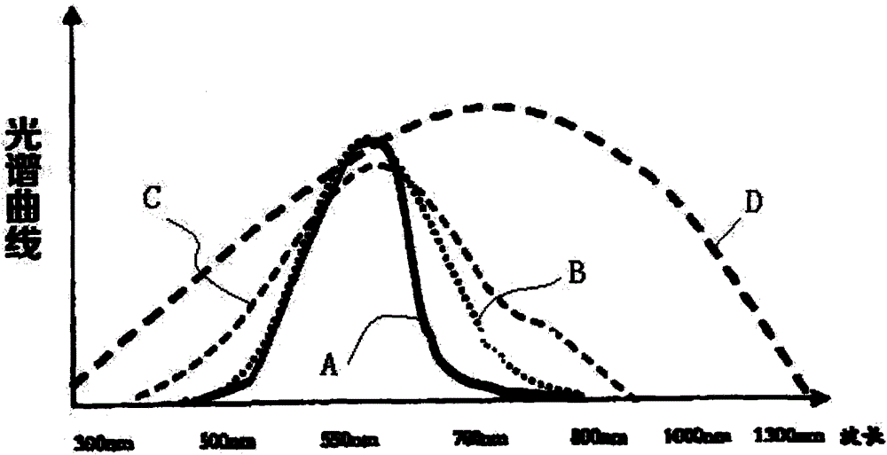
[0031] The following will be combined with figure 1 And attached figure 2 The present invention is further described, but it should not be used to limit the protection scope of the present invention.

[0032] The anti-infrared photosensitive receiving device packaging material of the present invention includes epoxy resin, curing agent, metal oxide and colorant; the epoxy resin is bisphenol A type epoxy resin, and the curing agent is methylhexahydro Phthalic anhydride, the metal oxide is WO , and the toner is yellow epoxy resin toner or orange epoxy toner. Based on the number of parts of bisphenol A epoxy resin: the number of parts of the bisphenol A epoxy resin is 80 to 95 parts; the number of parts of the methyl hexahydrophthalic anhydride is 90 to 99 parts ; The number of copies of WO3 is 0-20 parts; the number of copies of the colorant is 0-20 parts.

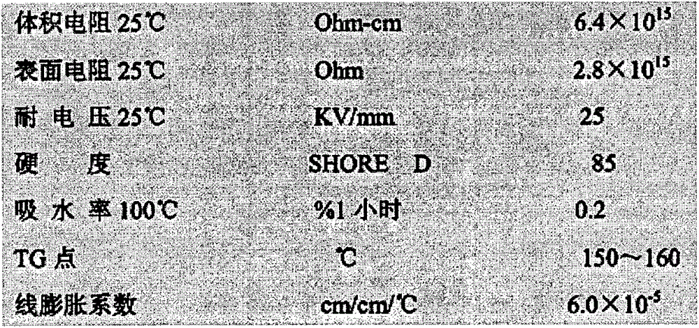
[0033] The specific technical indicators of the bisphenol A type epoxy resin, methyl hexahydrophthalic anhydride, WO3,...


PUM


Abstract

The invention discloses an anti-infrared photosensitive receiving device packaging material and a visible light sensor, and relates to the technical field of electronic packaging materials and visible light sensors. The packaging material includes epoxy resin and curing agent, and the anti-infrared photosensitive receiving device packaging material also includes metal oxide and toner; the epoxy resin is bisphenol A type epoxy resin, and the curing agent is Methyl hexahydrophthalic anhydride, the metal oxide is WO3, and the toner is yellow epoxy resin toner or orange epoxy toner. Based on the number of parts of bisphenol A epoxy resin: the number of parts of the bisphenol A epoxy resin is 80 to 95 parts; the number of parts of the methyl hexahydrophthalic anhydride is 90 to 99 parts ; The number of copies of WO3 is 0-20 parts; the number of copies of the colorant is 0-20 parts. The technology has good anti-infrared effect, high linearity, simple raw materials and low cost.

Description

technical field [0001] The invention relates to the technical field of electronic packaging materials and visible light sensors, in particular to a packaging material for an anti-infrared photosensitive receiver and a visible light sensor using the packaging material. Background technique [0002] A visible light sensor in the prior art is a sensor that can detect a spectrum similar to the range of the human eye. Such sensors mainly use silicon photodiodes, silicon phototransistors, etc. as detectors directly. Belonging to a single photoelectric sensor, the incident spectrum usually corresponds to a larger bandwidth (visible light to near infrared). For example: silicon photodiodes, triode products, incident wavelengths from 300nm to 1100nm, have photoelectric conversion effects in this range (see Figure A). And most of them don't have gain amplifier transistors. CdS photoresistor is the best visible light detector, but the production process of the product is complicated...

Claims


Application Information

Patent Timeline
IPC IPC(8): C08L63/00C08K3/22C08G59/42H01L31/0203H01L23/29
CPCH01L2224/48091H01L2224/48137H01L2224/48247H01L2924/00014
Inventor 吴晓龙吴胜
Owner 吴晓龙
Why Eureka
Try Eureka