Photocatalytic water splitting catalyzing structure and preparation method thereof
A manufacturing method and a technology for photolysis of water, applied in the field of photocatalysis, can solve the problems of not greatly improving, and achieve the effects of low cost, strong operability, and simple structure and process
- Summary
- Abstract
- Description
- Claims
- Application Information
AI Technical Summary
Problems solved by technology
Method used
Image
Examples
Embodiment 1
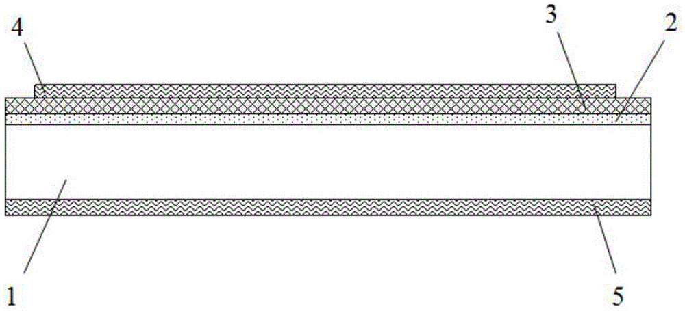
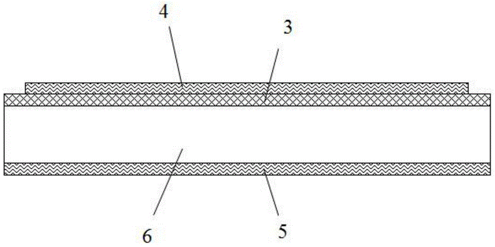
[0038] Please refer to figure 1 , figure 1 It is a schematic diagram of the structure of the photocatalytic water splitting of the present invention, such as figure 1 As shown, the photocatalytic structure of the present invention includes: a glass substrate 1; a conductive layer 2 located on the upper surface of the glass substrate 1 to form a conductive substrate, and the conductive layer 2 is fluorine-doped tin oxide or aluminum-doped oxide Zinc conductive film, the fluorine-doped tin oxide has a mass percentage of 5% fluorine or the aluminum-doped zinc oxide has an aluminum doping mass percentage of 8%, and the fluorine-doped tin oxide or aluminum-doped oxide The thickness of the zinc conductive film is 50nm; the photocatalyst layer 3 is located on the upper surface of the conductive layer 2, and the photocatalyst layer 3 is pure α-Fe 2 o 3, whose thickness is 200nm; and a cover layer, which includes an upper cover layer 4 and a lower cover layer 5, the upper cover laye...
Embodiment 2
[0051] Please refer to figure 1 , figure 1 It is a schematic diagram of the structure of the photocatalytic water splitting of the present invention, such as figure 1 As shown, the photocatalytic structure of the present invention includes: a glass substrate 1; a conductive layer 2 located on the upper surface of the glass substrate 1 to form a conductive substrate, and the conductive layer 2 is fluorine-doped tin oxide or aluminum-doped oxide Zinc conductive film, the fluorine-doped tin oxide has a mass percentage of 7% or the aluminum-doped zinc oxide has a mass percentage of 9%, and the fluorine-doped tin oxide or aluminum-doped oxide The thickness of the zinc conductive film is 120nm; the photocatalyst layer 3 is located on the upper surface of the conductive layer 2, and the photocatalyst layer 3 is pure α-Fe 2 o 3 , whose thickness is 300nm; and a cover layer, which includes an upper cover layer 4 and a lower cover layer 5, the upper cover layer 4 is located on the up...
Embodiment 3
[0064] Please refer to figure 1 , figure 1 It is a schematic diagram of the structure of the photocatalytic water splitting of the present invention, such as figure 1 As shown, the photocatalytic structure of the present invention includes: a glass substrate 1; a conductive layer 2 located on the upper surface of the glass substrate 1 to form a conductive substrate, and the conductive layer 2 is fluorine-doped tin oxide or aluminum-doped oxide Zinc conductive film, the fluorine-doped tin oxide has a mass percentage of 8% by mass or the aluminum-doped zinc oxide has an aluminum-doped mass percentage of 10%, and the fluorine-doped tin oxide or aluminum-doped oxide The thickness of the zinc conductive film is 200nm; the photocatalyst layer 3 is located on the upper surface of the conductive layer 2, and the photocatalyst layer 3 is pure α-Fe 2 o 3 , whose thickness is 400nm; and a covering layer, which includes an upper covering layer 4 and a lower covering layer 5, the upper ...
PUM
| Property | Measurement | Unit |
|---|---|---|
| thickness | aaaaa | aaaaa |
| thickness | aaaaa | aaaaa |
| thickness | aaaaa | aaaaa |
Abstract
Description
Claims
Application Information
 - Generate Ideas
- Intellectual Property
- Life Sciences
- Materials
- Tech Scout
- Unparalleled Data Quality
- Higher Quality Content
- 60% Fewer Hallucinations
Browse by: Latest US Patents, China's latest patents, Technical Efficacy Thesaurus, Application Domain, Technology Topic, Popular Technical Reports.
© 2025 PatSnap. All rights reserved.Legal|Privacy policy|Modern Slavery Act Transparency Statement|Sitemap|About US| Contact US: help@patsnap.com


