
Patsnap Eureka
For R&D, Patsnap Eureka makes reading and utilizing patents & technical documents easy.
Patsnap Eureka AIR
Designed for self-driven R&D workflows. Generate viable solutions, solve complex R&D challenges, empower your innovation with AI.

Patsnap Eureka Materials
Designed for material experts only. Revolutionize your material R&D, from search, analyze, to developing new materials.

TechResearch
Generate reliable direction feasibility study reports for your R&D in just a few steps.

TechSeek
Discover and master advanced knowledge NOW. Basics, ideas, possibilities, all at once.

TechMind
As an expert in R&D Theories, TechMind can generates customized viable solutions instantly.

TechRisk
Analyze your overall solution with one click, know your potential R&D risks in advance.

TechMonitor
Get weekly tech updates, stay abreast of the latest tech innovations and key insights.
Test method of FPGA chip application circuit
A test method and gate array technology, applied in the direction of detecting faulty computer hardware, etc., can solve problems such as not being able to achieve ideal results, and achieve the effects of reducing unknown faults, reducing difficulty, and reducing algorithm complexity
- Summary
- Abstract
- Description
- Claims
- Application Information
AI Technical Summary
Problems solved by technology
Method used
Image

Examples
Embodiment Construction
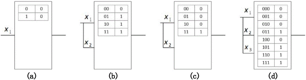
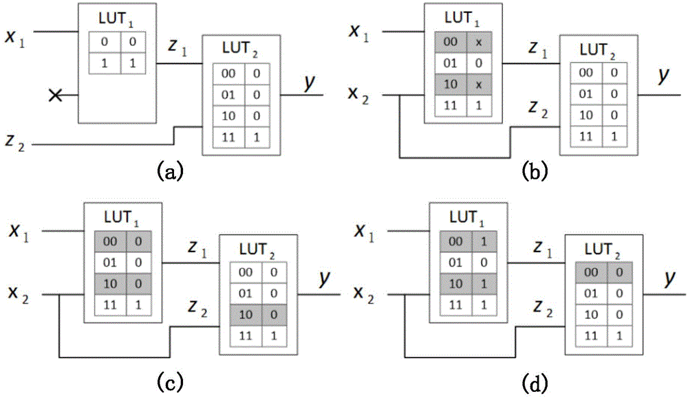
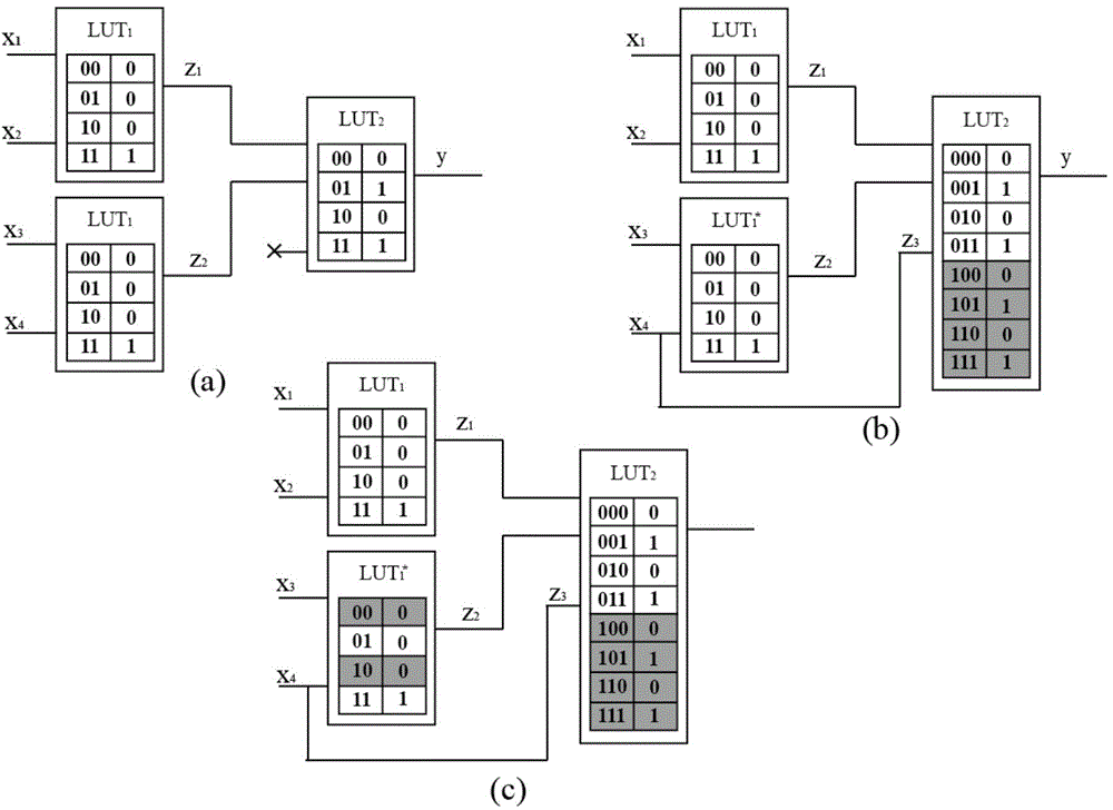
[0031] The method for testing an application circuit of a field programmable gate array chip of the present invention performs functional equivalent reconstruction on the LUT unit pair in the FPGA application circuit. When two directly connected LUT units meet certain constraints, by adding local redundant interconnection lines, the number of test vectors required for the local circuit can be reduced, thereby reducing the total test vectors required for the entire circuit as a whole number. The way of adding redundant interconnection lines can be divided into two types: forward redundant interconnection lines and backward redundant interconnection lines. Specifically include the following steps:
[0032] (1) Between the two directly connected look-up table units of the field programmable gate array chip application circuit, add a backward redundant interconnection line, and the adding method is as follows:
[0033] If two directly connected lookup table units meet the follow...
PUM
 Abstract
Description
Claims
Application Information
 - R&D Engineer
- R&D Manager
- IP Professional
- Industry Leading Data Capabilities
- Powerful AI technology
- Patent DNA Extraction
Browse by: Latest US Patents, China's latest patents, Technical Efficacy Thesaurus, Application Domain, Technology Topic, Popular Technical Reports.
© 2024 PatSnap. All rights reserved.Legal|Privacy policy|Modern Slavery Act Transparency Statement|Sitemap|About US| Contact US: help@patsnap.com