Antifuse structure and method of forming same
A technology of anti-fuse and isolation structure, which is applied in the direction of electrical components, electric solid-state devices, circuits, etc., can solve the problems of high programming voltage and difficulty in making high-voltage transistors, and achieve the effect of increasing process costs
- Summary
- Abstract
- Description
- Claims
- Application Information
AI Technical Summary
Problems solved by technology
Method used
Image
Examples
Embodiment Construction
[0026] In the process of forming MOS transistors using the existing CMOS process, because the thickness of the formed gate oxide layer is too low, it is easy to cause breakdown or leakage. Therefore, the thickness of the gate oxide layer corresponding to each process node is limited. will be reduced without limit. For the gate oxide antifuse, since the gate oxide layer needs to be broken down to activate the antifuse, a thicker gate oxide layer will result in a higher programming voltage for programming the gate oxide layer antifuse, which requires the use of A high voltage transistor generates the programming voltage. With the continuous decline of semiconductor process nodes, the manufacture of high-voltage transistors will become more and more difficult.
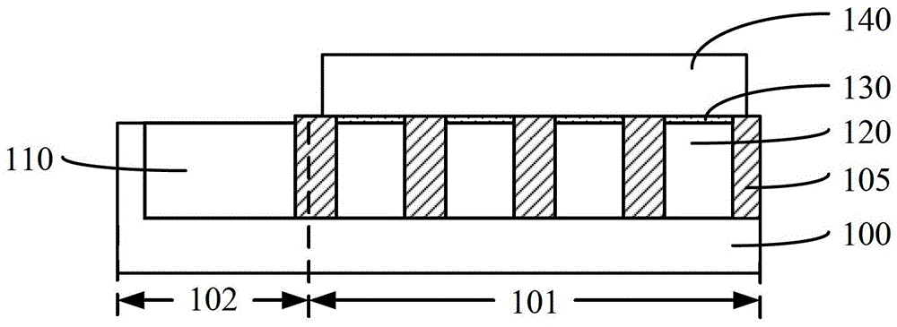
[0027] To this end, the inventors have proposed an antifuse structure and a method for forming the same. A gate oxide layer is formed on the entire surface of the active region surrounded by the shallow trench isolation ...
PUM
 Abstract
Description
Claims
Application Information
 - R&D
- Intellectual Property
- Life Sciences
- Materials
- Tech Scout
- Unparalleled Data Quality
- Higher Quality Content
- 60% Fewer Hallucinations
Browse by: Latest US Patents, China's latest patents, Technical Efficacy Thesaurus, Application Domain, Technology Topic, Popular Technical Reports.
© 2025 PatSnap. All rights reserved.Legal|Privacy policy|Modern Slavery Act Transparency Statement|Sitemap|About US| Contact US: help@patsnap.com


