
Through-hole design system

A design system and via technology, which is applied in computing, instrumentation, electrical digital data processing, etc., can solve problems such as long time, and achieve the effect of fast response speed

Inactive Publication Date: 2014-10-15
SCIENBIZIP CONSULTINGSHENZHENCO
View PDF6 Cites 6 Cited by
  • Summary
  • Abstract
  • Description
  • Claims
  • Application Information

AI Technical Summary

Problems solved by technology

In the prior art, 3D full-wave electromagnetic software is usually used for via hole simulation, which takes a relatively long time

Method used


Image

  • Through-hole design system
  • Through-hole design system
  • Through-hole design system

Examples


Embodiment Construction

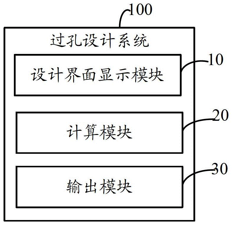
[0013] Please refer to figure 1 , the via design system 100 in this embodiment runs on a computing device (not shown), and the system 100 includes a design interface display module 10 , a computing module 20 and an output module 30 .

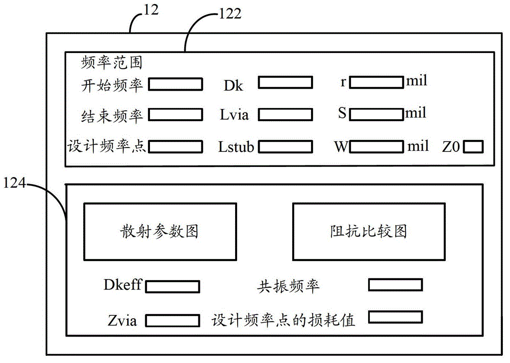
[0014] Please refer to figure 2 , the design interface display module 10 displays a via design interface 12 on the display device of the computing device. The interface 12 includes a parameter input area 122 and a result display area 124 . The parameter input area 122 is used to input various design parameters. In this embodiment, the various design parameters include the frequency range to be observed, the design frequency point, the dielectric coefficient Dk of the plate, the via length Lvia excluding the via stub, the length Lstub of the via stub, and the length of the via stub. Radius r, spacing S of differential vias, radius W of avoidance holes, and reference impedance Z0.

[0015] The calculation module 20 calculates the actual imped...


PUM


Abstract

The invention provides a through-hole design system which comprises a design interface display module, a calculating module and an output module, wherein the design interface display module is used for displaying a through-hole design interface on a calculating device; the interface comprises a parameter input area and a result display area; the parameter input area is used for inputting a to-be-observed frequency range, a design frequency point, a panel dielectric coefficient Dk, the length Lvia of the through hole excluding a through-hole remained section, the length Lstub of a through-hole remained section, radius r of the through hole, distance S of differential through holes, radius W of an avoiding hole and reference impedance Z0; the calculating module is used for calculating practical impedance Zvia and ideal impedance Zc of the through hole according to the parameter inputted to the parameter input area and a preset formula and drawing an impedance comparison diagram according to the calculated practical impedance Zvia and ideal impedance Zc; the output module is used for outputting the impedance comparison diagram to the result display area. After the through-hole design system provided by the invention is adopted, the response speed is high and a designer can quickly find the optimum design for the through hole according to the result displayed in the result display area.

Description

technical field [0001] The invention relates to the field of PCB design, in particular to a via hole design system. Background technique [0002] For PCBs, the most important thing to maintain signal integrity is impedance matching and consistent continuity. Impedance discontinuity will lead to the reflection of differential wire signals, and vias are an important factor leading to the discontinuity of differential wires. If the impedance of the via can be controlled to match the impedance of the differential wire, the signal reflection will be reduced, the quality of signal transmission will be improved, and the system will work stably. Therefore, when designing a PCB, it is necessary to simulate the via structure first to obtain the optimal via structure. In the prior art, 3D full-wave electromagnetic software is usually used for via hole simulation, which takes a relatively long time. Contents of the invention [0003] In view of this, the present invention improves ...

Claims


Application Information

Patent Timeline
IPC IPC(8): G06F17/50
Inventor 蔡昆宏
Owner SCIENBIZIP CONSULTINGSHENZHENCO
Learn More