Method for preparing vanadium dioxide film by using magnetron sputtering process
A vanadium dioxide and magnetron sputtering technology, applied in sputtering coating, metal material coating process, vacuum evaporation coating and other directions, can solve the range of small temperature change and phase transition temperature adjustment of vanadium dioxide film Narrow and other problems to achieve the effect of avoiding adverse effects
- Summary
- Abstract
- Description
- Claims
- Application Information
AI Technical Summary
Problems solved by technology
Method used
Image
Examples
preparation example Construction
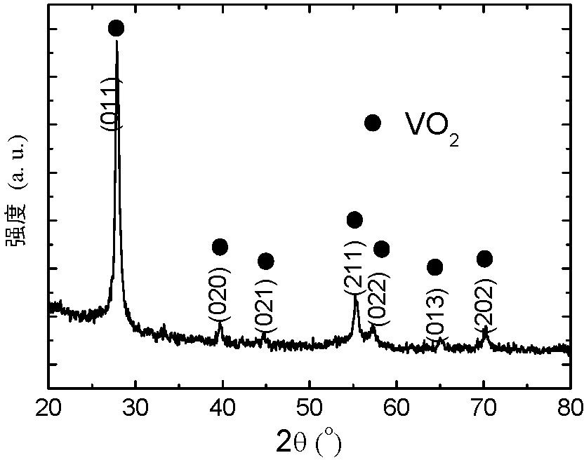
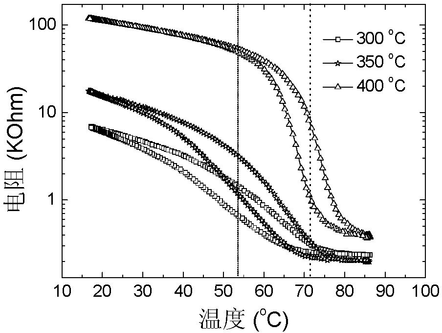
[0024]The preparation method of the present invention adopts a magnetron sputtering method, adopts a multifunctional magnetron sputtering system, uses a metal vanadium target, vacuumizes, controls the substrate temperature, and feeds argon and oxygen as sputtering gases respectively. and reactive gases to prepare VO 2 film. Specifically, a multifunctional magnetron sputtering system can be used, using high-purity metal vanadium (purity: 99.99%) as the target material, the target material diameter is 2 to 4 inches, the thickness is 4 to 6mm, and the background vacuum is 1 to 5×10 -5 Pa, the substrate temperature is 300-500°C, the Ar gas flow rate is 30-50 sccm, the sputtering power is 20-100w, the sputtering time is 60-300min, and the oxygen flow rate is 0.4-2 sccm.
[0025] The substrate can be selected as Na-free ordinary glass, quartz glass, sapphire or coated with a layer of SiN x Si substrate. For example, by plating a layer of SiN x The Si sheet is used as the substra...
Embodiment 1
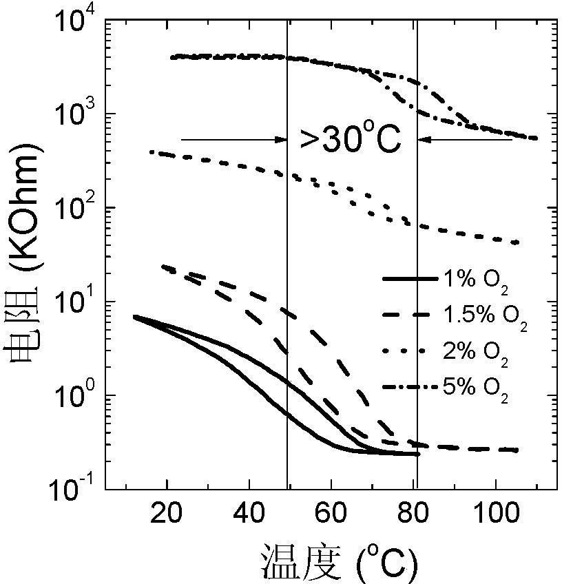
[0039] The substrate is a Si sheet coated with a layer of SiNx as the substrate. The SiNx layer is mainly an insulating layer to avoid the leakage of the film in the electrical test. It is cleaned by standard ultrasonic cleaning with acetone, ethanol and deionized water. Using a multi-functional magnetron sputtering system, using high-purity metal vanadium (purity: 99.99%) as the target, the target diameter is 2 inches, the thickness is 5mm, and the back vacuum is 3×10 -5 Pa, the deposition temperature is 400°C, the Ar gas flow rate is 40 standard condition milliliters per minute (sccm), the sputtering power is 60w, the sputtering time is 150min, and the oxygen flow rate is 0.4sccm (that is, the oxygen partial pressure is 1.0%). The grain size of the vanadium thin film is 15nm and the thickness is 70nm.
Embodiment 2
[0041] The steps of Example 1 were basically repeated, except that the oxygen flow rate was 0.6 sccm, that is, the oxygen partial pressure was 1.5%, and the particle size of the vanadium dioxide film was 18 nm, and the thickness was 70 nm.
PUM
| Property | Measurement | Unit |
|---|---|---|
| Thickness | aaaaa | aaaaa |
| Particle size | aaaaa | aaaaa |
| Thickness | aaaaa | aaaaa |
Abstract
Description
Claims
Application Information
 - R&D Engineer
- R&D Manager
- IP Professional
- Industry Leading Data Capabilities
- Powerful AI technology
- Patent DNA Extraction
Browse by: Latest US Patents, China's latest patents, Technical Efficacy Thesaurus, Application Domain, Technology Topic, Popular Technical Reports.
© 2024 PatSnap. All rights reserved.Legal|Privacy policy|Modern Slavery Act Transparency Statement|Sitemap|About US| Contact US: help@patsnap.com


