How to use the shared pad structure compatible with antenna soldering and thimble testing
A pad and antenna technology, applied in the field of shared pad structure, can solve the problem that the pad is not compatible with antenna welding and thimble testing functions at the same time, so as to improve production and testing efficiency, prevent tin connection phenomenon, and reduce occupancy. area effect
- Summary
- Abstract
- Description
- Claims
- Application Information
AI Technical Summary
Problems solved by technology
Method used
Image
Examples
Embodiment
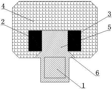
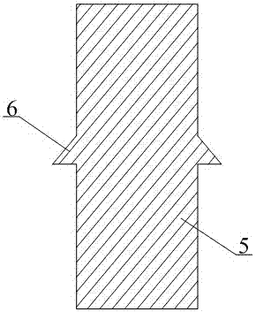
[0030] Such as figure 1 , 2 As shown, the present invention includes a first pad 1, a second pad 2, a third pad 3, a fourth pad 4 and a corresponding layer 5 for which copper is prohibited, and all components are arranged on the front or back of the PCB substrate . The second pad 2 and the third pad 3 are arranged symmetrically on the fourth pad 4 , and the first pad 1 is connected to the positive pole of the antenna and located outside the fourth pad 4 . The copper-forbidden corresponding layer 5 completely covers the surface of the first pad, and extends between the second pad 2 and the third pad 3, completely separating the second pad from the third pad. The so-called copper-forbidden corresponding layer means that copper is prohibited to be laid in this area, which is used as the adjacent ground between each pad, and is mainly used to prevent the WIFI signal from being affected. And the extended isolation part 6 between the first pad, the second pad and the third pad th...
PUM
 Abstract
Description
Claims
Application Information
 - R&D
- Intellectual Property
- Life Sciences
- Materials
- Tech Scout
- Unparalleled Data Quality
- Higher Quality Content
- 60% Fewer Hallucinations
Browse by: Latest US Patents, China's latest patents, Technical Efficacy Thesaurus, Application Domain, Technology Topic, Popular Technical Reports.
© 2025 PatSnap. All rights reserved.Legal|Privacy policy|Modern Slavery Act Transparency Statement|Sitemap|About US| Contact US: help@patsnap.com


