
Image processing method and electronic device

An electronic device and image processing technology, which is applied in the field of image processing, can solve problems such as heavy computing pressure, and achieve the effects of improving timeliness, reducing the amount of computing, and reducing noise

Active Publication Date: 2014-09-24
LENOVO (BEIJING) LTD
View PDF6 Cites 24 Cited by
  • Summary
  • Abstract
  • Description
  • Claims
  • Application Information

AI Technical Summary

Problems solved by technology

[0005] This application provides an image processing method and an electronic device, which are used to solve the problem in the prior art that image registration causes a large computing pressure on the hardware when multi-frame image fusion is used for noise reduction, and realizes the The unit records the camera motion parameters, and then quickly registers multiple frames of images according to the motion parameters

Method used


Image

  • Image processing method and electronic device
  • Image processing method and electronic device
  • Image processing method and electronic device

Examples


Embodiment 1

[0032]The present application provides an image processing method through Embodiment 1, which is applied to an electronic device. The electronic device includes an image acquisition unit and a motion sensing unit, and the motion sensing unit is used to detect motion parameters of the image acquisition unit. Specifically, the electronic device can be a digital camera, a digital video camera, a smart phone, a tablet computer, a smart watch, smart glasses, etc., the image acquisition unit is a camera, and its photosensitive element can be a charge-coupled device (English: Charge-coupled Device; Abbreviation: CCD), or complementary metal oxide semiconductor (English: Complementary Metal Oxide Semiconductor; abbreviation: CMOS), or other photosensitive components capable of photosensitive imaging. The motion sensing unit can be an acceleration sensor, a gyroscope, a gravity sensor, a rotation vector sensor, etc., which can be implemented based on hardware or software. In addition, t...

Embodiment 2

[0089] Corresponding to the image processing method in Embodiment 1, the present application provides an electronic device through Embodiment 2, the electronic device includes an image acquisition unit and a motion sensing unit, and the motion sensing unit is used to detect the movement of the image acquisition unit parameters; see Figure 5 , the electronic equipment includes:

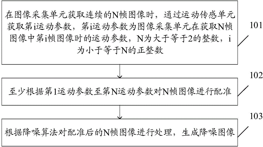
[0090] The motion parameter acquisition module 10 is used to obtain the i-th motion parameter through the motion sensing unit when the image acquisition unit acquires continuous N frames of images, and the i-th motion parameter is when the image acquisition unit acquires the i-th frame of images in the N frames of images motion parameters, N is an integer greater than or equal to 2, and i is a positive integer less than or equal to N;

[0091] A registration module 20, configured to register N frames of images at least according to the first motion parameter to the Nth motion parameter;

[0092] The...


PUM


Abstract

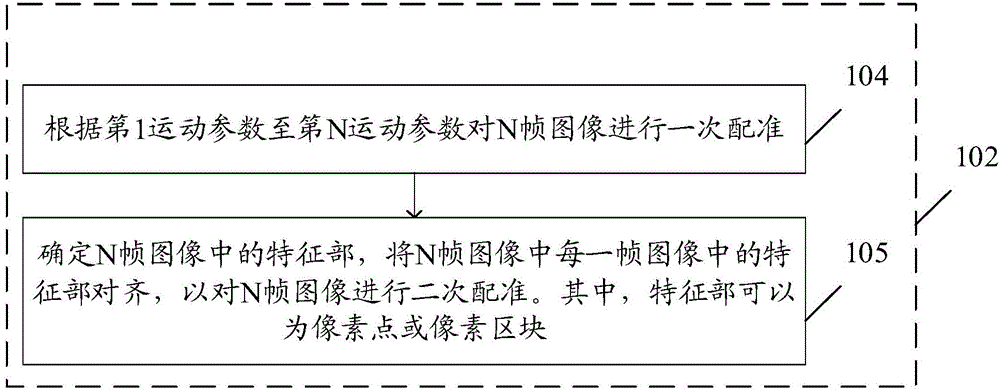
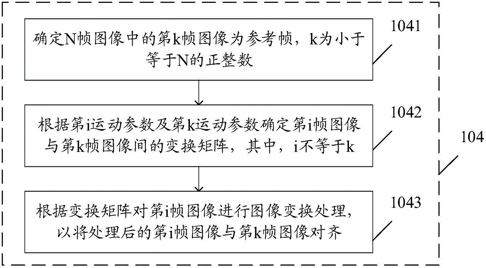
The invention discloses an image processing method and an electronic device to solve the problem of the prior art that high operational pressure is caused to hardware by image registration during noise reduction by means of fusion of multiple frames of images. The method is applied to the electronic device. The electronic device comprises an image acquisition unit and a motion sensing unit, wherein the motion sensing unit is used for detecting the motion parameters of the image acquisition unit. The method comprises the steps of acquiring the ith motion parameter through the motion sensing unit when the image acquisition unit acquires N frames of continuous images, wherein the ith motion parameter is obtained when the image acquisition unit acquires the ith frame of image in the N frames of images, N is an integer larger than or equal to 2, and i is a positive integer smaller than or equal to N; conducting registration on the N frames of images at least according to the first motion parameter to the Nth motion parameter; processing the N frames of images obtained after registration according to the noise reduction algorithm to enable a noise reduction image to be generated.

Description

technical field [0001] The invention relates to the field of image processing, in particular to an image processing method and an electronic device. Background technique [0002] With the rapid development of digital image acquisition technology, not only digital cameras, digital video cameras and other image acquisition devices have become popular, but also devices such as smart phones, tablet computers, smart watches and other devices can also have good image acquisition functions. However, due to the limited size of the photosensitive element in the device, the photosensitive area of ​​a single pixel is relatively small, and the number of photons that can be received per unit time is limited, resulting in insufficient exposure of photos in low-light environments and poor imaging effects. [0003] At present, there are two ways to solve this problem: first, prolong the exposure time, so that the photosensitive element can get enough light input, which can produce an output...

Claims


Application Information

Patent Timeline
Patent Type & Authority Applications(China)
IPC IPC(8): H04N5/217H04N5/232
Inventor 胡娜张帆
Owner LENOVO (BEIJING) LTD
Learn More