
Digital holographic three-dimensional appearance detecting device based on multiple wavelengths

A digital holography and three-dimensional topography technology, applied in measurement devices, optical devices, instruments, etc., can solve problems such as wavelength limitation and limited application range, and achieve the effect of ensuring measurement accuracy, improving measurement range, and reducing exposure times.

Inactive Publication Date: 2014-08-27
BEIHANG UNIV
View PDF4 Cites 22 Cited by
  • Summary
  • Abstract
  • Description
  • Claims
  • Application Information

AI Technical Summary

Problems solved by technology

[0003] In order to apply digital holography technology to the shape detection of planar 3D objects with large height and high roughness, some technical problems need to be solved: (1) The 3D shape detection of digital holography is limited by the wavelength, and the measurement range is only the wavelength. In order to improve the measurement range, the phase unwrapping technology is generally used, but this technology is limited by the surface topography of the object, and it can only perform phase unwrapping on a specific surface, and its application range is very limited

Method used


Image

  • Digital holographic three-dimensional appearance detecting device based on multiple wavelengths
  • Digital holographic three-dimensional appearance detecting device based on multiple wavelengths
  • Digital holographic three-dimensional appearance detecting device based on multiple wavelengths

Examples


Embodiment Construction

[0025] The present invention will be further described in detail with reference to the accompanying drawings and embodiments.

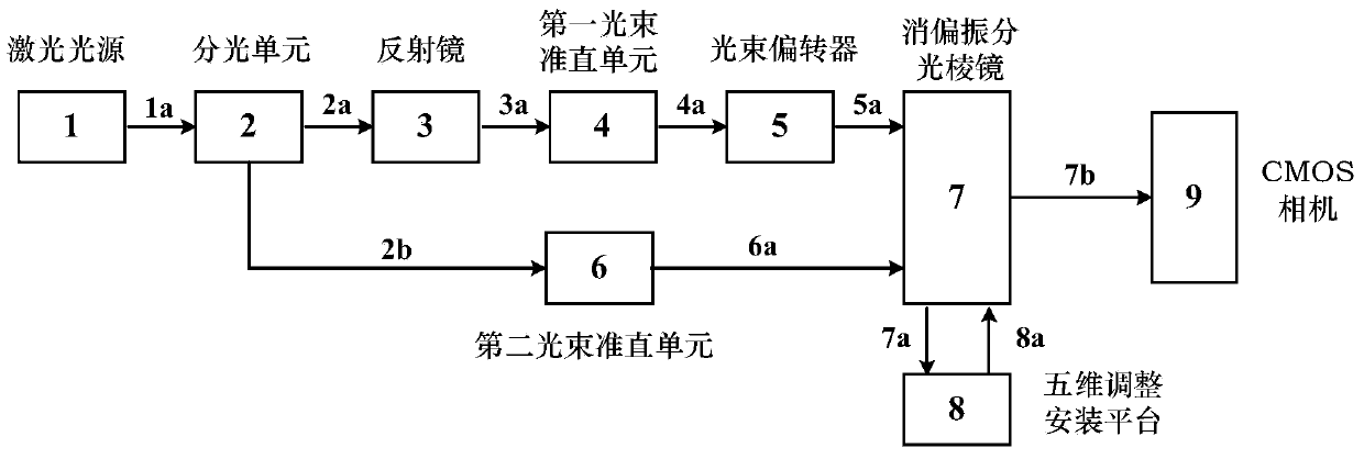
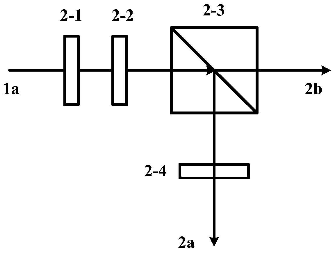
[0026] The present invention is a multi-wavelength digital holographic three-dimensional shape detection device, such as figure 1 As shown, it includes a laser light source 1, a beam splitting unit 2, a mirror 3, a first beam collimating unit 4, a beam deflector 5, a second beam collimating unit 6, a depolarizing beam splitting prism 7, a five-dimensional adjustment installation platform 8, CMOS camera9.

[0027] Wherein, the first beam collimating unit 4 and the second beam collimating unit 6 have the same structure.

[0028] The laser light source 1 generates laser light 1a, and the laser light 1a is input to the light splitting unit 2;

[0029] Laser light source 1 is used to provide 635nm-682nm laser 1a, that is, optical information. This light source provides a single longitudinal mode laser with a central wavelength range of 635nm-682nm. The m...


PUM


Abstract

The invention relates to a digital holographic three-dimensional appearance detecting device based on multiple wavelengths. The device carries out surface appearance measurement on the surface of a three-dimensional object by adopting the multiple wavelengths through a digital holographic method. In an optical path structure, the object to be measured is illuminated by planar optical waves, reflected object light is collected, and the included angle between reference light and the object light is controlled through a light beam deflector to achieve off-axis digital holography. In order to enlarge the measurement range while the observation resolution ratio is ensured, the object to be measured can be measured through light beams with the different wavelengths, obtained holographic spectrograms are processed in a subtractive iteration mode, and then three-dimensional appearance information of the object which is to be measured and free of phase position wrapping is obtained. Due to an integrated optical platform, all the optical elements are compact in layout structure, flexible to use and stable, and the detecting device can be used for observing three-dimensional appearances of optical elements large in height and high in accuracy and roughness and mechanical assemblies including mechanical rotors and the like on line.

Description

technical field [0001] The invention relates to a multi-wavelength-based digital holographic three-dimensional shape detection device, which belongs to the technical field of photoelectric measurement. Background technique [0002] At present, the three-dimensional shape detection technology mainly includes speckle interference technology, structured light technology and digital holography technology. Digital holography technology uses CCD, CMOS and other photoelectric image sensor devices to record holograms in digital form, and uses computer numerical simulation of optical diffraction process to reproduce the wavefront distribution of the original light field, so as to accurately obtain the amplitude and phase information of the object to be measured. [0003] In order to apply digital holography technology to the shape detection of planar 3D objects with large height and high roughness, some technical problems need to be solved: (1) The 3D shape detection of digital holog...

Claims


Application Information

Patent Timeline
Patent Type & Authority Applications(China)
IPC IPC(8): G01B11/24
Inventor 潘锋肖文陈宗晖闫贝贝杨洪建赵晨晓张旭红
Owner BEIHANG UNIV
Learn More