Metal interconnect structure and method of manufacturing the same

A technology of metal interconnection structure and manufacturing method, which is applied in semiconductor/solid-state device manufacturing, electrical components, electrical solid-state devices, etc., can solve the problems of high mechanical strength requirements of CNT through holes, achieve guaranteed density, facilitate high-density growth, Improve the effect of high density

Active Publication Date: 2016-06-22
SHANGHAI HUALI MICROELECTRONICS CORP
View PDF3 Cites 0 Cited by
  • Summary
  • Abstract
  • Description
  • Claims
  • Application Information

AI Technical Summary

Problems solved by technology

one is Figure 1A The process (a) shown in this process (a) uses catalyst particles (catalyst particles) as the growth source in advance, and relies on the guidance of the electric field to form vertical CNTs on the interconnection layer Metal1, and form CNT through holes between adjacent CNTs and CNTs. (via), and then use the CVD method to form a deposited dielectric layer, which is equivalent to epitaxially growing a uniform thickness catalytic epitaxial layer (blanketcatalystfilm) SiO in the through hole 2 , and then form the interconnection layer Metal2, whose defect is that the mechanical strength of the CNT through hole is relatively high; the other is Figure 1B The process (b) shown in the process (b) is similar to the traditional single damascene, in which the catalyst particle (catalyst particle) is used as the growth source in the dielectric layer via (via) that has been formed, relying on the crowding effect (crowding- effect), so that CNTs grow vertically in the through holes of the dielectric layer, but the defect is that the density of CNTs grown by this process is lower than that of CNTs grown by process (a)

Method used


Image

  • Metal interconnect structure and method of manufacturing the same
  • Metal interconnect structure and method of manufacturing the same
  • Metal interconnect structure and method of manufacturing the same

Examples


Embodiment Construction

[0032] In order to make the object and features of the present invention more obvious and easy to understand, the specific embodiments of the present invention will be further described below in conjunction with the accompanying drawings. However, the present invention can be realized in different forms, and should not be considered as being limited to the described embodiments .

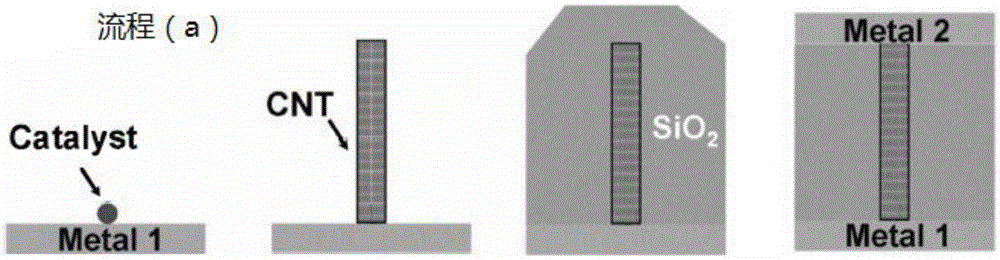
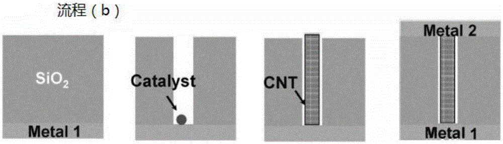
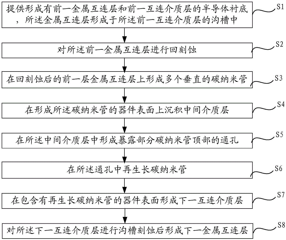
[0033] Please refer to figure 2 , the present invention proposes a method for manufacturing a metal interconnection structure, comprising the following steps:

[0034] S1, providing a semiconductor substrate formed with a previous metal interconnect layer and a previous interconnect dielectric layer, the metal interconnect layer is formed in the trench of the previous interconnect dielectric layer;

[0035] S2, etching back the previous metal interconnection layer;

[0036] S3, forming a plurality of vertical carbon nanotubes on the previous metal interconnection layer after etching back;

[003...


PUM


Abstract

The invention provides a metal interconnection structure and a manufacture method thereof. The growth area of a carbon nano tube is increased through a groove, formed through etching, of a previous metal interconnection layer, high-density growth of the carbon nano tube is facilitated, the formed high-density carbon nanao tube can serve as a growth source of a regenerated carbon nano tube in a subsequent through hole, density of the regenerated carbon nano tube in the through hole is improved, and accordingly the density of the carbon nano tubes growing from through holes is guaranteed and performance of the metal interconnection structure is improved.

Description

technical field [0001] The invention relates to the field of semiconductor manufacturing, in particular to a metal interconnection structure and a manufacturing method thereof. Background technique [0002] With the further shrinking of the critical dimensions of copper interconnection, it is difficult to meet the electrical requirements by relying solely on copper as a conductor, so researchers have begun to experiment with some new materials to replace copper. [0003] Carbon nanotubes (CNTs) are currently used as a potential replacement material for copper interconnects, which can significantly reduce wire resistance and do not suffer from electromigration, but how to integrate CNTs into copper interconnects is a big challenge. [0004] Please refer to Figure 1A with 1B , two feasible integration processes are proposed in the prior art (TowardsFutureVLSIInterconnectsUsingAlignedCarbonNanotubes, 2011IEEE), but both face their own problems. one is Figure 1A The process ...

Claims


Application Information

Patent Timeline
Patent Type & Authority Patents(China)
IPC IPC(8): H01L21/768H01L23/532
Inventor 鲍宇
Owner SHANGHAI HUALI MICROELECTRONICS CORP
Why Eureka
Try Eureka