Wafer-level zoom lens module and manufacturing method thereof
A zoom lens, wafer-level technology, applied in nonlinear optics, instruments, optics, etc., to achieve the effect of convenient specification
- Summary
- Abstract
- Description
- Claims
- Application Information
AI Technical Summary
Problems solved by technology
Method used
Image
Examples
Embodiment 1
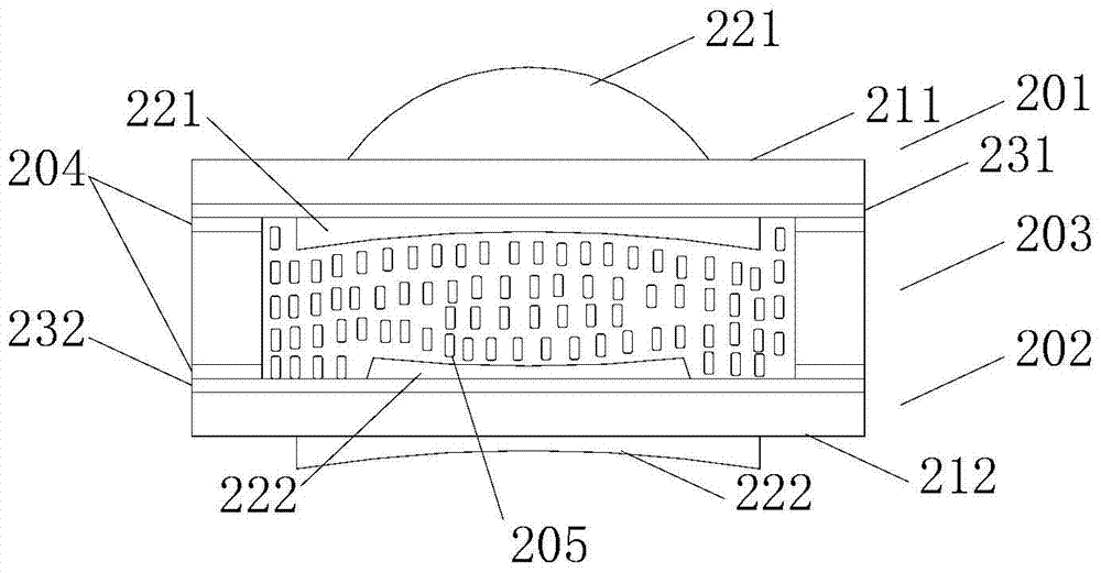
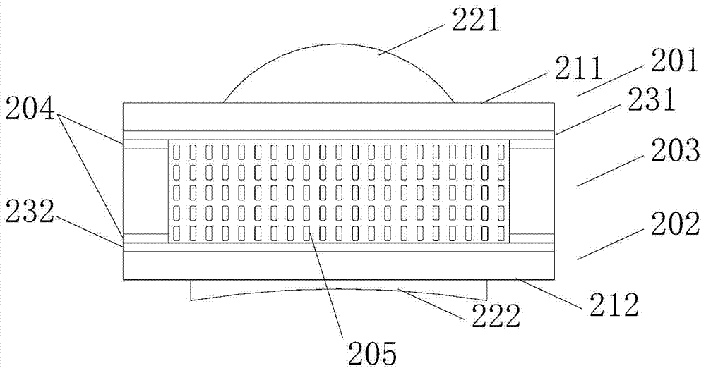
[0076] Such as Figure 2A-2B As shown, the wafer-level zoom lens module in this embodiment includes: a first lens layer 201 and a second lens layer 202 , and a spacer layer 203 located between the first lens layer 201 and the second lens layer 202 . The first lens layer 201 includes a first transparent conductive glass substrate 211, at least one first lens 221 and a first transparent conductive film 231; the second lens layer 202 includes a second transparent conductive glass substrate 212, at least one second lens 222 and the second transparent conductive film 232; one of the surfaces of the first transparent conductive glass substrate 211 is covered with the first transparent conductive film 231, similarly, one of the surfaces of the second transparent conductive glass substrate 212 is covered with the second transparent conductive film 232 . The first lens 221 and the second lens 222 are both plano-convex lenses or plano-concave lenses, that is, lenses with a plane surfac...
Embodiment 2
[0082] Because the wafer-level zoom lens module in the present invention is not limited to two layers of lens layers, it can also include three layers or more than three layers of lens layers. The structure of the lens module above the lens layer is roughly similar, therefore, in this embodiment, a lens module with three lens layers is taken as an example for detailed description.
[0083] Such as image 3 As shown, the wafer-level zoom lens module in this embodiment includes: a top wafer layer 301 at the top of the lens module, a middle lens layer 302 at the middle of the lens module, a bottom lens layer 303 at the bottom of the lens module and A plurality of spacer layers 301 located between every two adjacent lens layers. The arrangement of the top lens layer 301 and the bottom lens layer 303 is the same as that of the first lens layer 301 and the second lens layer 302 in Embodiment 1, so details will not be repeated here. The middle lens layer 302 in this embodiment incl...
PUM
| Property | Measurement | Unit |
|---|---|---|
| thickness | aaaaa | aaaaa |
Abstract
Description
Claims
Application Information
 - Generate Ideas
- Intellectual Property
- Life Sciences
- Materials
- Tech Scout
- Unparalleled Data Quality
- Higher Quality Content
- 60% Fewer Hallucinations
Browse by: Latest US Patents, China's latest patents, Technical Efficacy Thesaurus, Application Domain, Technology Topic, Popular Technical Reports.
© 2025 PatSnap. All rights reserved.Legal|Privacy policy|Modern Slavery Act Transparency Statement|Sitemap|About US| Contact US: help@patsnap.com


