High-power semiconductor laser beam combining method
A laser beam combining and semiconductor technology, applied in the field of laser applications, can solve the problems of limited application fields, inability to apply lasers, and large loss of light energy, and achieve the effect of being beneficial to application, low cost, and low loss of light energy
- Summary
- Abstract
- Description
- Claims
- Application Information
AI Technical Summary
Problems solved by technology
Method used
Image

Examples
Embodiment 1
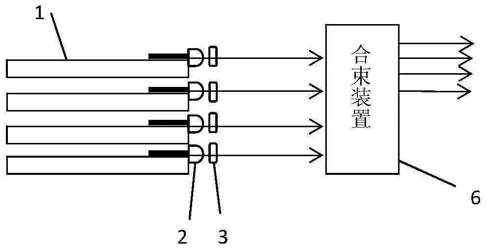
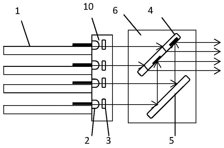
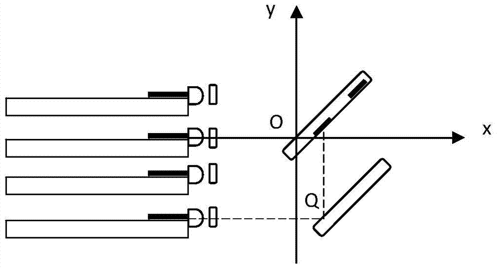
[0057] Figure 2aIt is a schematic diagram of the optical path of a high-power semiconductor laser beam combiner combined with the method of the present invention. A high-power semiconductor laser beam combining device includes a semiconductor laser stack 1, a collimating lens group 10, and a beam combining system 6 arranged sequentially along the optical path. The semiconductor laser stack 1 is composed of 4 groups of semiconductor laser unit stacks. The combining Beam system 6 comprises a reflective spacer film layer mirror 4 and a total reflection mirror 5, and described reflective spacer film layer mirror 4 is to plate reflective film at intervals on the lower surface of flat lens, and the quantity of reflective film is 2, and the spacing of reflective film and The width of itself is equal; the reflective spacer film layer mirror 4 and the total reflection mirror 5 are placed between the light emitting direction of the semiconductor laser stack 1 at 45°, and correspond to ...
Embodiment 2
[0073] Figure 3a An embodiment of a semiconductor laser beam combining system designed for combining the beam combining method of the present invention. The laser beam combining system is mainly composed of a semiconductor laser stack 1, a collimating lens group 10 and a beam combining system 6. The semiconductor laser stack 1 is composed of 4 semiconductor laser units; the collimating lens group is placed on the semiconductor The laser laser exit place includes a fast-axis collimating lens 2 and a slow-axis collimating array 3, wherein the fast-axis collimating lens can be a collimating D-type aspherical lens; the slow-axis collimating array is a single array cylindrical lens; The beam combining system 6 is placed in the outgoing direction of the collimated laser beam, and is composed of two parallelepiped prisms 7. The two parallelepiped prisms 7 are placed parallel to each other at equal intervals, and the placement positions are fixed in the vertical direction in turn. S...
Embodiment 3
[0086] Figure 5 An embodiment of a semiconductor laser beam combining system designed in conjunction with the beam combining method of the present invention, a high-power semiconductor laser beam combining system includes a semiconductor laser array 1, a collimating lens group 10 and a beam combining device arranged in sequence along the optical path 6. The collimating lens group 10 includes a fast-axis collimating lens 2 and a slow-axis collimating array 3, wherein the fast-axis collimating lens is a collimating D-type aspheric lens, and the slow-axis collimating array is a single-array cylinder lens. The small prism in the prism combination in the beam combiner 6 is selected from a triangular prism 8, and the included angle between the acute angles of two adjacent sides of the parallelepiped prism 9 is 45°. The semiconductor laser stack is divided into upper and lower parts. For example, the semiconductor laser stack 1 includes 4 semiconductor laser units, the upper 2 semi...
PUM
 Abstract
Description
Claims
Application Information
 - R&D
- Intellectual Property
- Life Sciences
- Materials
- Tech Scout
- Unparalleled Data Quality
- Higher Quality Content
- 60% Fewer Hallucinations
Browse by: Latest US Patents, China's latest patents, Technical Efficacy Thesaurus, Application Domain, Technology Topic, Popular Technical Reports.
© 2025 PatSnap. All rights reserved.Legal|Privacy policy|Modern Slavery Act Transparency Statement|Sitemap|About US| Contact US: help@patsnap.com