
Preparation method for gate oxide

A gate oxide layer and oxidation process technology, which is applied in semiconductor/solid-state device manufacturing, electrical components, semiconductor devices, etc., can solve the problem that the thermal oxidation process cannot improve the interface state in a timely and effective manner, and reduce the possibility of generating interface states. , the effect of stabilizing nitrogen content, improving life and performance

Inactive Publication Date: 2014-07-23
SHANGHAI HUALI MICROELECTRONICS CORP
View PDF3 Cites 2 Cited by
  • Summary
  • Abstract
  • Description
  • Claims
  • Application Information

AI Technical Summary

Problems solved by technology

However, since the semiconductor technology entered the 45nm era, the traditional method of improving the interface state of the gate oxide film has encountered unprecedented challenges, that is, the thermal oxidation treatment process after film formation cannot effectively improve the interface state in a timely manner.

Method used


Image

  • Preparation method for gate oxide

Examples


Embodiment Construction

[0022] The present invention will be described in further detail below in conjunction with the accompanying drawings and specific embodiments. Advantages and features of the present invention will be apparent from the following description and claims. It should be noted that the drawings are all in very simplified form and use imprecise ratios, which are only used to facilitate and clearly assist the purpose of illustrating the embodiments of the present invention.

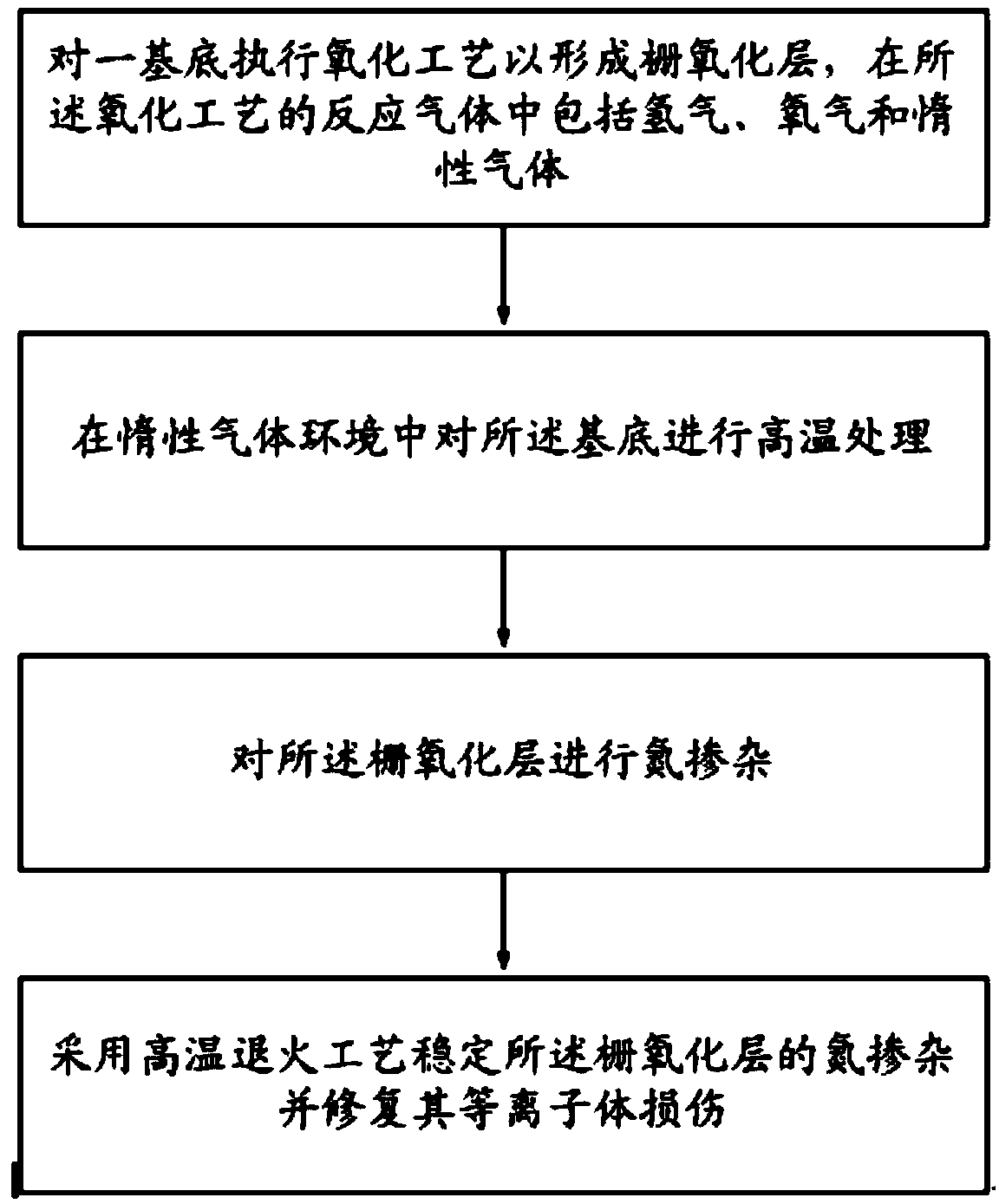
[0023] Such as figure 1 As shown, the preparation method of the gate oxide layer provided by the present invention comprises the following steps:

[0024] S1: performing an oxidation process on a substrate to form a gate oxide layer, wherein a reaction gas in the oxidation process includes an inert gas.

[0025] Among them, the oxidation process described is in-situ water vapor generation (ISSG). ISSG is a new low-pressure rapid oxidation thermal annealing technology, which is currently mainly used in the growth...


PUM


Abstract

The invention provides a preparation method for gate oxide. Inert gas is used for attenuating hydrogen in reaction gas to reduce the number of Si-H bonds and S-O-H bonds generated on an Si-SiO2 interface, high-temperature treatment is performed on a substrate after an oxidation film is formed to accelerate stress releasing of the inside structure of the oxidation film so that the possibility of generating an interface state because of rupture bonds generated nearby the interface can be reduced. By the adoption of the method, total charge of the interface state of the gate oxide can be effectively reduced by at least one order of magnitude, and because the gate oxide has stable nitrogen content, service life of components can be prolonged, and performance of the components can be improved.

Description

technical field [0001] The invention relates to the technical field of semiconductor manufacturing, in particular to a method for preparing a gate oxide layer. Background technique [0002] With the shrinking of the size of semiconductor devices, the thickness of the gate oxide layer used in high-performance logic devices is required to be less than 2nm, which leads to a series of problems such as interface trap charges, gate dielectric tunneling leakage current and reliability. These problems are considered to some extent related to the presence of incompletely oxidized Si atoms in the film or to the Si-SiO 2 It is related to the interface state existing at the interface. [0003] There are two main reasons for the generation of interface states: [0004] 1. Mechanism based on hydrogen bond model. This mechanism holds that Si-SiO 2 The hydrogen-bonded structure near the interface is detached from the hydrogen atoms due to the capture of the kinetic energy of the inciden...

Claims


Application Information

Patent Timeline
Patent Type & Authority Applications(China)
IPC IPC(8): H01L21/28
CPCH01L21/28H01L21/0223H01L21/02318
Inventor 张红伟
Owner SHANGHAI HUALI MICROELECTRONICS CORP
Learn More