


Quick Research
Generate reliable direction feasibility study reports for your R&D in just a few steps.

Technical Q&A
Discover and master advanced knowledge NOW. Basics, ideas, possibilities, all at once.

Find Solutions
As an expert in R&D theories, this can generate solutions to your technical problems instantly.

Evaluate Feasibility
Analyze your overall solution with one click, know your potential R&D risks in advance.

Monitor Landscape
Get weekly tech updates, stay abreast of the latest tech innovations and key insights.
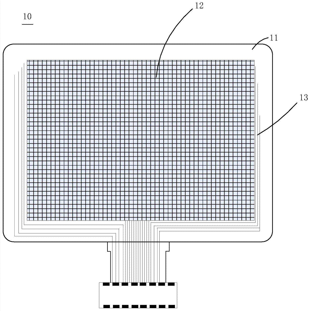
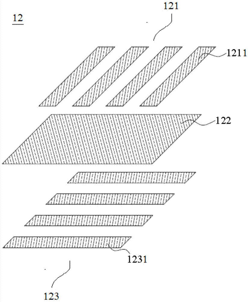
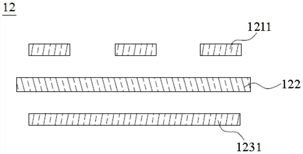
Biometric feature recognition sensor and electronic equipment comprising same
A biometric feature recognition and sensor technology, applied in character and pattern recognition, instruments, computer components, etc., can solve the problems of reducing the resolution of fingerprint recognition sensors, inability to perform fingerprint recognition accurately, and increasing the cost of fingerprint recognition equipment, etc., to achieve improved Effects of bonding yield, length reduction, and increase in the number of electrodes
- Summary
- Abstract
- Description
- Claims
- Application Information
AI Technical Summary
Problems solved by technology
Method used
Image

Examples
Embodiment Construction
[0028] Example embodiments will now be described more fully with reference to the accompanying drawings. Example embodiments may, however, be embodied in many forms and should not be construed as limited to the embodiments set forth herein; rather, these embodiments are provided so that this disclosure will be thorough and complete, and will fully convey the concept of example embodiments to those skilled in the art. The same reference numerals denote the same or similar structures in the drawings, and thus their repeated descriptions will be omitted.
[0029] The described features, structures, or characteristics may be combined in any suitable manner in one or more embodiments. In the following description, numerous specific details are provided in order to give a thorough understanding of embodiments of the invention. However, those skilled in the art will appreciate that the technical solutions of the present invention may be practiced without one or more of the specific...
PUM
 Abstract
Description
Claims
Application Information
 - R&D Engineer
- R&D Manager
- IP Professional
- Industry Leading Data Capabilities
- Powerful AI technology
- Patent DNA Extraction
Browse by: Latest US Patents, China's latest patents, Technical Efficacy Thesaurus, Application Domain, Technology Topic, Popular Technical Reports.
© 2024 PatSnap. All rights reserved.Legal|Privacy policy|Modern Slavery Act Transparency Statement|Sitemap|About US| Contact US: help@patsnap.com