Solar battery manufacturing method
A technology for solar cells and manufacturing methods, which is applied in the direction of final product manufacturing, sustainable manufacturing/processing, circuits, etc., can solve the problems of low utilization rate of epitaxial wafers, waste of edges and corners, etc., to increase the production process flow, improve the utilization rate, The effect of increasing production costs
- Summary
- Abstract
- Description
- Claims
- Application Information
AI Technical Summary
Problems solved by technology
Method used
Image
Examples
Embodiment 1
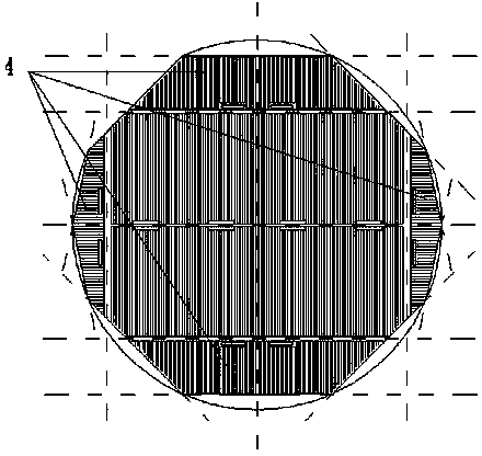
[0038] Such as figure 2 Shown is a schematic structural diagram of a solar cell formed in an embodiment of the present invention. According to the method for manufacturing solar cells by utilizing the corner regions of epitaxial wafers provided by the present invention, grid lines and electrodes are manufactured in the sub-cell regions, and small-sized solar cells of triangular, trapezoidal or other shapes are manufactured by dicing.
[0039] specifically, figure 2 The shown solar cell size of the main solar cell region is 30mm×40mm solar cell or 40mm×60mm solar cell, which forms four secondary solar cell regions 4 by using the corner regions.
Embodiment 2
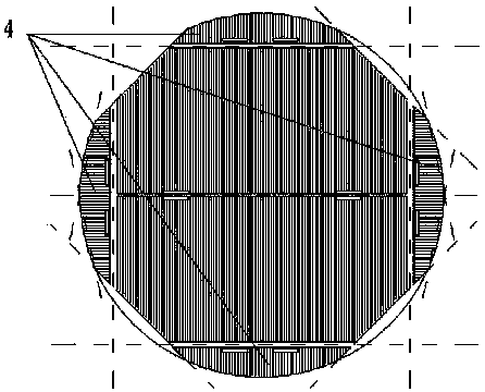
[0041] Such as image 3 Shown is a schematic structural view of a solar cell formed in another embodiment of the present invention. According to the method for manufacturing solar cells by utilizing the corner regions of epitaxial wafers provided by the present invention, grid lines and electrodes are manufactured in the sub-cell regions, and small-sized solar cells of triangular, trapezoidal or other shapes are manufactured by dicing.
[0042] specifically, image 3 The solar cell size of the shown main solar cell area is 40mm×80mm or 80mm×80mm solar cell, which forms four secondary solar cell areas 4 by using the corner areas.
[0043] In summary, the solar cells involved in the present invention are manufactured from the corners of the epitaxial wafers. By using the method of using the corners of the epitaxial wafers, the utilization rate of the epitaxial wafers can be improved without increasing the process flow and production of solar cells. cost, achieving cost reducti...
PUM
 Abstract
Description
Claims
Application Information
 - R&D
- Intellectual Property
- Life Sciences
- Materials
- Tech Scout
- Unparalleled Data Quality
- Higher Quality Content
- 60% Fewer Hallucinations
Browse by: Latest US Patents, China's latest patents, Technical Efficacy Thesaurus, Application Domain, Technology Topic, Popular Technical Reports.
© 2025 PatSnap. All rights reserved.Legal|Privacy policy|Modern Slavery Act Transparency Statement|Sitemap|About US| Contact US: help@patsnap.com


