Method for growing graphene by controlling graphene nucleation loci on substrate

A nucleation site, graphene technology, applied in graphene, semiconductor/solid-state device manufacturing, electrical components, etc., can solve the problem of uncontrollable graphene nucleation sites, strange shapes, and difficulty in becoming large in size, etc. question

Inactive Publication Date: 2014-07-16
FUDAN UNIV
View PDF5 Cites 6 Cited by
  • Summary
  • Abstract
  • Description
  • Claims
  • Application Information

AI Technical Summary

Problems solved by technology

However, during the growth process, the nucleation sites of graphene on the copper substrate are uncontrollable. Some places on the copper have nucleation sites, and some places have no nucleation sites. The graphene grown in this way is discontinuous and has a shape of Very strange, the area is also difficult to become very large

Method used


Image

  • Method for growing graphene by controlling graphene nucleation loci on substrate
  • Method for growing graphene by controlling graphene nucleation loci on substrate
  • Method for growing graphene by controlling graphene nucleation loci on substrate

Examples


Embodiment Construction

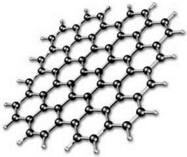
[0018] The present invention controls and prepares graphene nucleation sites on the substrate, and can directly grow a continuous graphene sample with a specific shape on the metal or insulator substrate by low-pressure chemical vapor deposition on the substrate. The method for growing graphene by controlling graphene nucleation sites on the substrate is reliable, the process steps are simple, convenient and reliable, and can be grown on a metal or insulator substrate, and the grown graphene can be controlled. The following is an example of using the graphene nucleation sites on the control substrate to grow graphene proposed by the present invention.

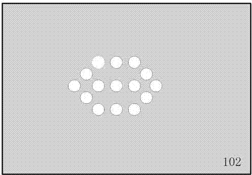
[0019] In the figure, for convenience of description, the structure size and ratio do not represent the actual size.

[0020] First, polish the copper (Cu) substrate or 300nm silicon dioxide (SiO2) 101 substrate to make the surface clean, smooth and flat. Next, clean the substrate sample to remove impurities, particles, residual re...


PUM


Abstract

The invention belongs to the technical field of carbon-based integrated circuit manufacturing and particularly provides a method for growing graphene by controlling graphene nucleation loci on a substrate. According to the method, the continuous graphene of various shapes grows on the copper or silicon dioxide substrate by controlling the graphene nucleation loci on the substrate, a mask plate with the shape well designed is utilized, and the physical vapor deposition method is used for depositing small dotted copper on the substrate to serve as the graphene nucleation loci, so that the graphene grows into the continuous grahene of specific shapes by controlling the nucleation loci. The method is simple, convenient to use, reliable and capable of being used as a basic method for growing the graphene through low-pressure chemical vapor deposition.

Description

Technical field [0001] The invention belongs to the technical field of carbon-based integrated circuit manufacturing, and specifically relates to a method for growing graphene on a substrate. Background technique [0002] With the invention of the first integrated circuit, the integrated circuit and semiconductor industries have experienced rapid development, and they are increasingly playing an important role in promoting the rapid development of science and technology. However, the continuous extension and depth of Moore's Law makes silicon-based integrated circuit devices closer and closer to their physical limits. With the discovery of a new type of semiconductor material-Graphene, it has brought unlimited development possibilities to the semiconductor industry in the future. Graphene is a honeycomb two-dimensional crystal composed of a single layer of hexagonal cell carbon atoms. figure 1 Shown is a schematic diagram of the basic structure of graphene. Graphene has a much ...

Claims


Application Information

Patent Timeline
IPC IPC(8): H01L21/205C01B31/04C01B32/186
CPCH01L21/02414C01B32/186H01L21/02491H01L21/02527H01L21/0262
Inventor 周鹏杨松波沈于兰
Owner FUDAN UNIV
Why Eureka
Try Eureka