Semiconductor device manufacturing method and stacked chip manufacturing method
A semiconductor and device technology, applied in the field of semiconductor preparation, can solve the problems of high cost, complicated preparation process, and low production capacity, and achieve the effects of increasing production capacity, simplifying the preparation process, and reducing costs
- Summary
- Abstract
- Description
- Claims
- Application Information
AI Technical Summary
Problems solved by technology
Method used
Image

Examples
preparation example Construction
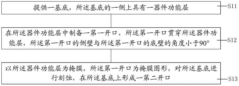
[0047] The core idea of the present invention is to provide a method for manufacturing a semiconductor device, including the following steps:
[0048] Step S11: providing a substrate with a device function layer on one side of the substrate;
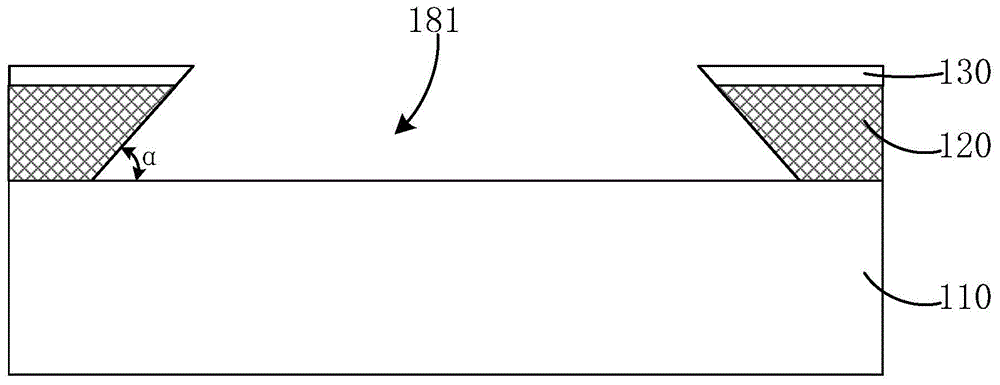
[0049] Step S12: Prepare a first opening in the device functional layer, the first opening penetrates the device functional layer, and the angle between the side wall of the first opening and the bottom wall of the first opening is less than 90 °;
[0050] Step S13: Using the device functional layer as a mask, and the first opening as a mask pattern, etching the substrate to form a second opening on the substrate.
[0051] The angle between the side wall of the first opening and the bottom wall of the first opening is less than 90°, so that the size of the top of the first opening is smaller than the size of the bottom of the first opening. In the second opening, the first opening is used as a mask pattern of the second opening, and the subst...
no. 1 example
[0058] Combine the following Figure 1-Figure 5 The semiconductor manufacturing method in this embodiment is described. among them, figure 1 Is a flowchart of the semiconductor manufacturing method of the first embodiment of the present invention; Figure 2-Figure 5 It is a schematic diagram of the structure of the semiconductor manufacturing method in the manufacturing process of the first embodiment of the present invention.
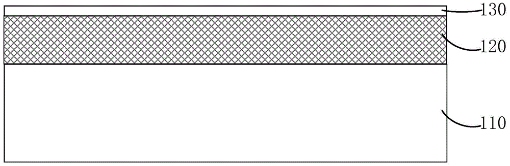
[0059] In the semiconductor manufacturing method of this embodiment, first, step S11 is performed to provide a substrate 110 with a device function layer 120 on one side of the substrate 110, such as figure 2 Shown. Among them, in figure 2 The material of the substrate 110 and the device function layer 120 are different. In other embodiments of the present invention, the material of the substrate 110 and the device function layer 120 may be the same or the same layer.
[0060] Preferably, before step S12, the method further includes forming a first barrie...
no. 2 example
[0065] See Figure 6-Figure 13 The preparation method of the stacked chip in this embodiment is described. among them, Image 6 Is a flow chart of the method for manufacturing a stacked chip according to the second embodiment of the present invention; Figure 7-Figure 13 It is a schematic diagram of the structure of the stacking chip manufacturing method in the manufacturing process of the second embodiment of the present invention. The method for preparing the stacked chip of the second embodiment uses the method of the first embodiment to prepare the second opening, and the specific steps are as follows:
[0066] First, proceed to step S21 to provide a first chip 200 and a second chip 300, such as Figure 7 As shown, the first chip 200 includes a first substrate 210 and a first epitaxial layer 220 on one side of the first substrate 210, and the first epitaxial layer 220 includes a first interconnect structure 221. The second chip 300 includes a second substrate 310 and a second...
PUM
 Abstract
Description
Claims
Application Information
 - R&D
- Intellectual Property
- Life Sciences
- Materials
- Tech Scout
- Unparalleled Data Quality
- Higher Quality Content
- 60% Fewer Hallucinations
Browse by: Latest US Patents, China's latest patents, Technical Efficacy Thesaurus, Application Domain, Technology Topic, Popular Technical Reports.
© 2025 PatSnap. All rights reserved.Legal|Privacy policy|Modern Slavery Act Transparency Statement|Sitemap|About US| Contact US: help@patsnap.com