Substrate etching method
A technology of substrate and etching depth, which is applied in the field of microelectronics, can solve the problems of pollution particles, lower product yield, complicated etching steps, etc., and achieve the effect of simple etching steps and lower manufacturing costs
- Summary
- Abstract
- Description
- Claims
- Application Information
AI Technical Summary
Problems solved by technology
Method used
Image
Examples
Embodiment Construction
[0044] In order for those skilled in the art to better understand the technical solution of the present invention, the substrate etching method provided by the present invention will be described in detail below in conjunction with the accompanying drawings.
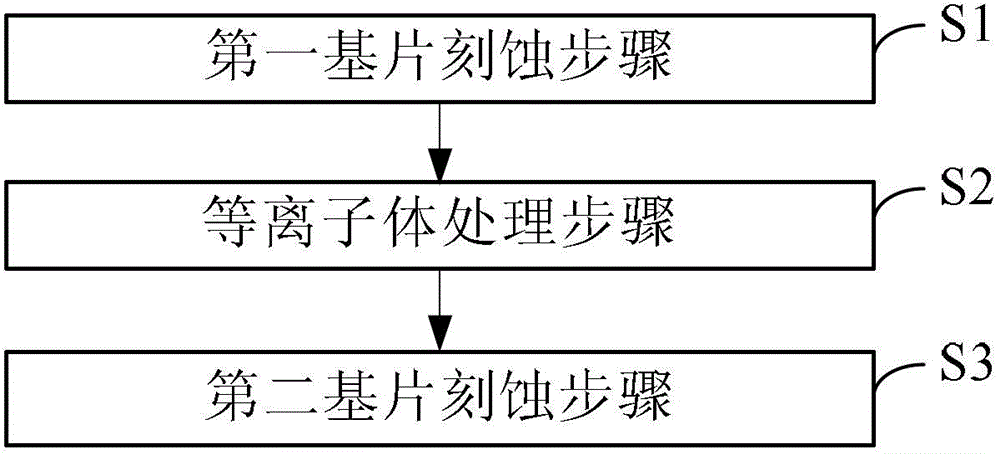
[0045] image 3 A flow chart of the substrate etching method provided by the present invention. see image 3 , the method is to divide the substrate etching process into two substrate etching steps, namely: the first substrate etching step and the second substrate etching step, and between the two, that is, after completing the first substrate etching step After the step, and before performing the second substrate etching step, a plasma treatment step is performed. Specifically, the following steps are included:
[0046] Step S1, the first substrate etching step. In step S1, an etching gas is fed into the reaction chamber, and an excitation power supply and a bias power supply are turned on, so as to etch the substra...
PUM
 Abstract
Description
Claims
Application Information
 - R&D Engineer
- R&D Manager
- IP Professional
- Industry Leading Data Capabilities
- Powerful AI technology
- Patent DNA Extraction
Browse by: Latest US Patents, China's latest patents, Technical Efficacy Thesaurus, Application Domain, Technology Topic, Popular Technical Reports.
© 2024 PatSnap. All rights reserved.Legal|Privacy policy|Modern Slavery Act Transparency Statement|Sitemap|About US| Contact US: help@patsnap.com


